Hugo Holden
Veteran Member
Hugo,
To answer your questions.
1. Nivag's board just maps ROM and/or RAM either external (using the PETs) or internal. There is a data bus buffer involved (or similar) so the PETs data bus is isolated from the internal bus. The (previously working) test was with internal ROM and RAM. Flipping the RAM link over causes PET RAM to be used instead of internal.
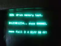
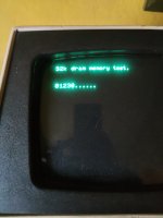
2. The PETTESTERs DRAM test is a slightly modified MARCH-C memory test. By slightly modified I have added two tests. One to clear memory to all $00 and validate this. The other to preset memory to all $FF and to validate this. Technically, these tests are performed by the MARCH-C tests anyhow. The MARCH-C memory tests are a recognised high coverage test for dynamic RAM devices. The only thing that I am planning to add to these tests in Version 5 is an inherent 'delay' between the $00 and $FF writing and validating steps to ensure the DRAM refresh circuitry is performing it's job.
However, there is a slight 'niggle' with my MARCH-C test. It uses both page 0 RAM and the stack (page 1 RAM) and relies on this working... I have a (too simple) memory test for pages 0 and 1 of the RAM before I use them in anger. I have found that some marginal RAM failures can pass the simple tests but cause the full memory test to crash (or malfunction). This malfunctioning has already been observed on Desperado's PET (it was reporting address $01FF in error - but it never tests this address!).
I have found a more comprehensive (but simple) memory test that I can use for my pages 0 and 1 testing in Version 5.
Dave
Yes, it is quite a different system.
Mine relies on dynamically deactivating the lower 1k or 2k (selectible) of DRAM and simultaneously activating a substitute SRAM to support BASIC, leaving the PET's CPU running normally and BASIC functioning. The firmware in my ROM, which is block moved into the functioning SRAM area, writes a checkerboard pattern and a reverse checkerboard pattern or any other chosen byte value, to test the DRAM, the latter can be useful tracking down defective DRAM.
Because of the delay it takes to do this, fill the memory (even with a machine language program), and then visually inspect the memory with the TIM, it also allows the refresh system (data retention) to be checked by default.
I did it this way because I stumbled across a vintage computer article with a program for DRAM checking, where there was a concern by the designers about a value in a memory cell changing, when an adjacent cell was written to, hence the reverse checkerboard pattern being needed. Though, they did not offer a scientific explanation as to how that could happen inside the IC, but it seemed plausible. So I thought I'd better pay attention to it. If there is one thing I have learnt about DRAM IC's, they are very complex devices and have a number of interesting failure modes and they rely on a lot of extra support circuitry that SRAM does not require.
") ...
...