• Please review our updated Terms and Rules here

CP/M on NVRAM?

Looks like I will be doing some reading and researching. The 4-megabit (512K x 8) 5-volt Only 256-byte Sector Flash Memory one does look very inviting though. 256 byte sectors.... That could be a good fit for my project; that would work well in an 8 bit system where I have the lower byte (of 3 bytes) just for that purpose.
Beware of terminology when reading the specs. The term "sector" is often used to define the smallest unit of ERASE. "page" is typically used to define the largest (or required) chunk of contiguous (and aligned) data to be written/programmed. The AT28C040 does have a 256-byte *page* size, and can only erase the entire chip.
 
Isn't the AT28C0x0 16 bit? The AT29C040 is 8 bit but will erase and write a single sector though it can also perform a chip-wide erase as well. The Winbond version W29C040 will also do the same.

The biggest difference in the datasheet I noticed is that on the 28cXXX you can rewrite individual bytes, while the 29c0X0 requires you to rewrite the entire page, or it will erase unwritten locations regardless of previous contents.
The AT28Cxxx series are 8-bit wide, 8-bit databus. And while they allow you to change a single byte in a page, you still have to operate it as a page device. Again, "page" not "sector".
 
Well, I see that the 29Cxxx datasheets do use the term "sector" in the way that the 28Cxxx datasheet uses "page". I suspect that is not accidental, and represents the difference in the technology. So, one should still beware of using the terms interchangeably. The 29Cxxx requires a whole "sector" to be written and programmed, while the 28Cxxx have a "page buffer" that allows arbitrary bytes (within the page) to be written without changing the rest.
 
It's like it was made for CP/M... And at 256K, it's the perfect size :) And they are DPID and cost $1 each....

I mean, I guess if that sounds like it's a thing you want I guess that's great, but I will just chuck this out there: A way-bigger-than-you-could-ever-need CF or SD card plus an adapter is about... $20, $25? They support LBA, which makes them easy to address, and if you really don't want to deal with sector blocking/deblocking (which from what I've seen in the CP/M disk driver code isn't that big of a deal) you could just use 128 bytes per sector. Sure, you're throwing away three quarters of the card, but who cares? I see Samsung Evo 32GB SD cards on Amazon for $7, that's less than a dollar per gigabyte even if you only use a quarter of it. Even if we allow that the card plus an adapter will be $25... heck, let's make it a nice round $32 to allow for the GAL, buffer, and sprinkling of resistors and decoupling caps it'll take to interface it to a Z-80 bus, that's $4 a gigabyte for more storage than CP/M could ever, ever use. (By a couple of orders of magnitude.) That makes it a dollar for 256 megabytes vs 256 kilobytes, or one thousand times cheaper, than rolling your own flash disk.

These devices are great for replacing a system ROM (IE, where you need random "read mostly" access but want the option to update in-place), but they're going to make terrible general purpose disks. The datasheet says a write cycle can take as much as 10 milliseconds; that's in the ballpark of floppy slow, nothing like a RAMdisk. Which, again, I guess will be fine if the only thing you want to use this for is a dedicated virtual floppy to load your OS into memory from, but if I were going to do that I'd probably try to engineer it as simply as possible, IE, a really nongranular page-flipper that'd reserve the first chunk of the ROM for the actual bootstrap ROM and for the disk portion just do some phat block moves through a bounce buffer, I wouldn't build an elaborate sector pager around it.
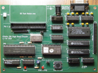
The only reason I am even thinking of doing it; is because I can. The CPU card in my STD system has a built in serial port and IDE as it is.....
1679253405821.png

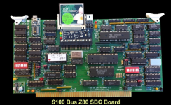
But my next project is going to be purely S-100 based. I'm thinking of the possibility of using this:
1679253523511.png

Hey, it's all fun and games, until a bit flips!
 
Hey, by all means doing it "because you can" is all the reason you need. ;)

Again, mostly I'm just noting that things like EEPROMs and small sector-rewritable flash chips aren't really aimed at being either (general purpose) disk replacements nor NVRAMs. (Being too slow, small, and wear-outable to be good for replacing disks, at least when it comes to writes, and not really behaving like RAM in the latter case. If you did somehow cook up an automatic memory controller for a AT28Cxxx that would stall the CPU whenever you did a write to wait for it to be committed to the chip you'd ruin it in seconds if you had something like the CPU stack in it, in addition to showing the machine to a crawl. A real battery-powered NVRAM would of course fine with that.) They are sometimes used in things like data-loggers where they get written "periodically", but usually those use an algorithm that walks linearly through the chip writing timestamped records until hitting the end, at which point it rolls over, to spread the wear as evenly as possible.
 
I read about this topic somewhat late and discussion went off into Flash hardware. I have a working battery-backed CP/M-ready Z80 SBC, Z80SBC64, designed over 5 years ago. It is a small 2"x4" ROMless design with 4 banks of 32KRAM where one bank contains the bootstrap software that's accessible immediatly after power on and then protected from inadvertent data corruption. CP/M 2.2 and CP/M 3 are ported to this hardware. A small monitor is located at 0xB400 away from CP/M's BDOS/CCP/BIOS and not conflicted with most CP/M software, so it can load BDOS/CCP/BIOS and load CP/M applications and start CP/M. In fact this is how it created the first file on a new CF disk by load and save XMODEM.COM.

The software is backed up when power is off so it can resume after power is re-applied; what I'm trying to figure out is how to pause and then resume CP/M software operation. CP/M software are generally not design for resumption so do you have one in mind? I can power up my Z80SBC64 again and try out such software.
Bill
 
I mean, I guess if that sounds like it's a thing you want I guess that's great, but I will just chuck this out there: A way-bigger-than-you-could-ever-need CF or SD card plus an adapter is about... $20, $25? They support LBA, which makes them easy to address, and if you really don't want to deal with sector blocking/deblocking

They do better than that - They support direct access mode for up to 9 and a bit bits of address line - and you can change down to the byte level... But I'm having a heck of a time trying to find an adapter that supported more than 3 address lines that are required in LBA mode - If you know of a full CF adapter, please let me know.

- edit: By "full adapter" I mean something that goes to 0.1" headers, or similar, rather than the CF socket with tiny little surface mount wires.
 
Last edited:
I read about this topic somewhat late and discussion went off into Flash hardware. I have a working battery-backed CP/M-ready Z80 SBC, Z80SBC64, designed over 5 years ago. It is a small 2"x4" ROMless design with 4 banks of 32KRAM where one bank contains the bootstrap software that's accessible immediatly after power on and then protected from inadvertent data corruption. CP/M 2.2 and CP/M 3 are ported to this hardware. A small monitor is located at 0xB400 away from CP/M's BDOS/CCP/BIOS and not conflicted with most CP/M software, so it can load BDOS/CCP/BIOS and load CP/M applications and start CP/M. In fact this is how it created the first file on a new CF disk by load and save XMODEM.COM.

The software is backed up when power is off so it can resume after power is re-applied; what I'm trying to figure out is how to pause and then resume CP/M software operation. CP/M software are generally not design for resumption so do you have one in mind? I can power up my Z80SBC64 again and try out such software.
Bill

Usually you save the state of the CPU and other devices in memory somewhere - eg, state tables. It's fairly commonly used in z80 in "Snapshot" devices like the Multiface that interrupt the processor, save all of the registers and the system memory to a file as an image, then restore operation.

Later you can load the snapshot and everything should come back the same, though things like disk controllers can complicate the issue as the state of a register controlled by an I/O port may not be so easy to snapshot.

The easiest way around this is to have the FDOS record this state somewhere in memory when it changes, eg, using the scratchpad registers in the DPH to store track and sector of the disk controller, and any other relevant state data... Even then, there should be a mechanism to restore this as otherwise if snapshotted in the middle of a disk operation, the outcome will usually result in a failure since the state doesn't get restored. Ideally, the restore should be carried out by the system software that will at least set the default disk and re-establish the sector and track data prior to handing control back to the snapshotted applications.
 
- edit: By "full adapter" I mean something that goes to 0.1" headers, or similar, rather than the CF socket with tiny little surface mount wires.

I'm not sure why such a thing would exist? The "memory" mode is exclusive to CF (well, technically it's a subset of PCMCIA); IDE simply doesn't have pins defined for those additional address lines. (And doesn't have any spare pins for them.)

Sparkfun used to sell a CF breakout board that took you from a CF socket to a 0.1" header, but they haven't for a few years, presumably because CF is kind of dead.

They support direct access mode for up to 9 and a bit bits of address line - and you can change down to the byte level..

Are you absolutely positive about that? I was kind of under the impression that their memory mode was kind of "fake". Here's a passage from a Sandisk manual:

3. Accesses to even addresses between 400h and 7FFh access register 8. Accesses to odd addresses between 400h and
7FFh access register 9. This 1 KByte memory window to the data register is provided so that hosts can perform
memory to memory block moves to the data register when the register lies in memory space.
Some hosts, such as the X86 processors, must increment both the source and destination addresses when executing the
memory to memory block move instruction. Some PCMCIA socket adapters also have auto incrementing address logic
embedded within them. This address window allows these hosts and adapters to function efficiently.

Note that this entire window accesses the Data Register FIFO and does not allow random access to the data buffer
within the CompactFlash Memory Card.

See that last part? IE, I'm pretty sure I read once that the address lines mostly just work for selecting the device registers; when it comes to the data window the first read inside of it gives you the first word and increments a counter so the next gives you the next, etc. Do you have an example of someone successfully doing random access I/O inside of that window? Every 8-bit CF interface I've ever seen treats it as IDE mode. (And I'm pretty sure they do this because there really isn't an advantage to memory mode.)
 
Last edited:
No, I am not sure, and I have no examples, and I've never tried myself - but unless I can get hold of a CF card adapter that supports A0 to A10, then it makes it a whole lot more difficult to find out... Though the way it's going, with all adapters I've found being IDE type ( for True IDE mode ) I have no easy way of buying an existing adapter and testing...

And due to the fine pins, challenges getting just the adapter without a PCB, etc, I'd really prefer to find an existing adapter and wire it up for testing -

So if you ever come across one, please let me know :)

Thanks
David
 
Back
Top