• Please review our updated Terms and Rules here

IBM 5110/5100 video Display card repair (possible diode fix)

voidstar78

Veteran Member
Joined
May 25, 2021
Messages
690
Location
Texas
I have two 5110's and one of them has a Display card issue. I know it is the Display card, because I can swap in the Display card from the good 5110 and it boots right up. (and the Bad Display card inserted into the other 5110 causes the same issue as the original 5110 it came from)

With the "bad" Display card is inserted (in either system), when the system is started the red light at the front comes on, and the Audio buzzer emits a tone (the 5110 added a little speaker behind the CRT, an upgraded feature over the 5100). In the 5110 MAP, I came across this result being consistent with a bad display card. (however, as far as I can tell, the MAP doesn't call out the Audible alert)

1654990784538.png

I don't think it is the Exec ROS or Base I/O -- because I can take both of those and use them in another 5110 that is functional.
I don't think it is the Z3 cable or RESTART switch, because I can insert cards from the "good" 5110 into this "bad" 5110, and it starts up fine (so all the switches and cables should be fine).

That just leaves "Bad G2"... Which it says to see MAP 050. Well, MAP 050 refers to jumpers that set the Display card for different regions (countries). The type of Display card I have corresponds to the 3rd column below (with the 4 sets of 3 pins), and the jumpers I have are set to EBCDIC (U.S.). I'm not entirely sure what this does, as far as the Display is concerned (load different CRT fonts? change power/Hz requirements?). I could try each variation -- which I plan to try it eventually -- just to eliminate it as being the problem.

1654991380645.png

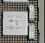
But a specific component on the board got my attention, which I'll explain the next post.
 
Last edited:
For context, here is what the two cards look like.

The "good" (working) one is at the Top. The "bad" (causes RED light and Audible alert on power up) one is at the Bottom.

In addition, the "GOOD" (top) one is from 1979. The "BAD" (bottom) one has components from late 1977 to early 1978. We know this because we've confirmed that the "rectangular standing up" components are resistor packs and are labeled (on the side) with the Year/Week of production. I measured most of these resistors, I don't think it is a resistor problem.

On the left side you see the jumpers at the MAP 050 refers to (where they are all set to the same side).

The main difference (that I see) is on the GOOD/upper Display card, there is a BLUE diode (I think it is a diode) around the center of the lower half. The OLD/lower Display card has --- something else (quite a different style diode).

IMG_2469A.jpg
 
Here (below) is that component in comparison across the two Display cards. The BLUE one (from the GOOD/Upper Display card) is possibly labeled "WS3" and "GR" (doesn't mean anything to me).

The other one, in the BAD/Lower Display card, is not labeled. [ note the two resistors in these images are installed in reverse order, which shouldn't matter, but just a noted inconsistency -- IMO it's evidence of "hand assembled" boards ]

Assuming these are both diodes, I used a Diode Tester on them. I'm not an expert about testing diodes, but my understanding is you connect the leads in both directions and assess the results. Which are: (yes, this is with the component still on the board...)

In the GOOD Display card (blue diode) [c.1979]

+/- --> .214v instantly and no voltage creep increase [ this is with the red positive lead on the side with the black mark ]
-/+ --> .196v instantly and no voltage creep increase

In the BAD Display card (red/clear component) [c.1977/78]

+/- --> started at .356v and increased gradually to .369v [ this is with the red positive lead on the side towards the silver can component ]
-/+ --> started from .280v and increased gradually to .319v

I'm not sure what that means, but there was no OL in either direction, and no major voltage delta. (maybe it's inconclusive with the component still being on the board?)


IMG_2477_compare_small.jpg
 
Last edited:
Sorry to be so long winded - but that's where I'm at. The chances of finding another 5110 Display card is slim (but if anyone knows of one, perhaps pulled from a system that isn't working), let me know. Meanwhile, any suggestions on things to check? (while I have a "good" working Display card to compare it with)
 
This is a tough one!

I think you are correct to isolate the problem to this card. Unfortunately, it is mystery meat to us right now, since we don't have a schematic and all of the components are identified with IBM aliases only.


I took a look at MAP 050 and there's not really a Procedure there, is there? It's a table of jumper settings. I suspect that the jumpers are unlikely to be the problem here: the vast majority of 5110s ever sold in the US will have been EBCDIC (US) models. One thing you might check, though: are the jumpers still "jumping"? That is, measure across the jumpers on the solder-side of the board and make sure that they're still (essentially) zero ohms; maybe you'll get lucky and find an oxide layer on the pins that, once cleared, gets everything working fine.

If that's not it, what would I do? Hmm...
I don't think the diode is the problem here, and the measurements you see (even with their differences) are likely to be artefacts of testing a diode in a circuit that has some bypass capacitors and other components on it. Maybe someone else might disagree! Anyway, I suppose I would do two things to start:


1. Using online resources (including ones we've linked to before), try to identify/understand the function of as many of these chips as possible. Hopefully we'll find that some of the DIPs are 74-series logic, for example. With this information, we'll begin to be able to piece together how this card is working, and from that, we might be able to determine a troubleshooting strategy.

If you can't find resources that identify a particular part number, consider comparing some of the components to ones on other cards you find in the 5110. It's likely that this card has a character ROM on it, for example: maybe we'll find that one of the "metal can" chips is similar to a different metal can chip that's obviously a ROM, like the ones on the non-executable ROS cards.


2. If we can, understand the process that delivers the error to us. It might be the case that the failure state (PROCESS CHECK light, buzzing noise) is triggered very early in the start-up process by the Executable ROS when it finds something it doesn't like about the display. I'd read through the start-up code and see if there's anything that stands out --- if we're lucky, we'll find that the code attempts to do something on the card and fails if that doesn't work. Then we can focus our troubleshooting to that particular process first.


Bonus, 3: Maybe your thermal camera can give us a hint. I'm guessing it's hard to get a clear view of the card while it's installed --- an extender board for the 5100/5110 would be useful! --- but maybe there's a way to see whether some component is getting unusually hot?
 
Good idea on checking the actual jumpers - they all check out, continuity top and bottom on both (good and "bad" Display card).

And good idea on checking the thermal image. But you're right, the Display card on the 5110 is wedged between the Processor and Common/Language ROS. So it'd be tricky to test -- such as from a cold start, run both for about 1min, remove the card, and check the thermal.


I recall something during my PSU project for the 5110: When I was dialing in the Amps of one of the rails (literally turning the Amp dial on one of those buck converters), I would cause the Audible alert (and red light) to go off. It may not have been the PSU itself causing that, but a side effect of something on the Display card "freaking out". Unfortunately, I can't recall which rail (might have been the -5v one, wish had better notes on that).... Now, I'm not saying this is a PSU problem (because putting in the GOOD Display does work). But from the perspective of this "BAD" Display card, maybe it is perceiving excessive Amps?


And some additional information: the BAD Display card actually does show stuff on the CRT! In REGISTER mode, it shows all "0" (abnormal). In regular mode, it shows a different symbol than 0 (something like an "8", like an hourglass or maybe two inverted triangles -- in any case, it is the same symbol across the entire display). BUT... then based on your idea #2.... I activated the STEP MODE!

The Audible alert doesn't happen until the 4th STEP. From the emulator work, I know the 5110 starts at whatever address is in the first 16-bit of the Executive ROS (000A in this case). And in your prior work, you found you can override this by intercepting the address loaded from that first two bytes. And a crazy peculiar thing about the 5100/5110 is that at the first startup moment, the screen is literally showing the contents of Executive ROS (so you can STEP right at startup, go to REGISTER mode, and reveal the Executive ROS 512-bytes at a time). But it's not code in the Executive ROS doing this -- that's why the emulators don't startup like this (I was going to modify mine to do this, just copy the first 512 bytes of execros.bin into RWS 0x200 at startup of the emulator -- haven't done that yet).

Anyhow, so the first 4 instructions of the Executive ROS startup should be...

000A 1FFF CTRL $F, #$FF ; Reset all devices
000C 0204 MOVE R2, R0
000E 8208 LBI R2, #$08 ; R2 <- $0008
0010 0324 MOVE R3, R2 <<< BEEP... when BAD Display is inserted (and screen goes blank, red light on, persistent audible alarm, system effectively halted)
0012 8300 LBI R3, #$00 ; R3 <- $0000
0014 5321 MOVE (R2)+, R3
0016 012C MHL R1, R2
0018 0126 OR R1, R2
001A C103 SZ R1
001C F009 BRA $0014 ; Loop

Not a lot of help - since I'm not sure how long the initial 1FFF takes (to reset all the devices), The next block of startup code (0010 to 001C) is a long loop (163824 cycles to be exact). Something like R2 is incremented (by 2) till it crosses FFFF and matches back to R1. I assume it is giving time for the devices to reset.... And the Display has a ROS that somehow communicates to get the ExecROS data and show it on the display (or maybe this is in some ISR?). The Audible Alarm (and all front panel stuff) is part of the Display device (so it can be self sufficient at issuing the lights and alarm).
 
There is a "trick" that you might be able to use, due to the fact you have a perfectly working card. Going out on a limb here...

Since the two cards, in the case that they were working perfectly, would have input and output signal that would agree with each other at least in the less than 10 or 30nS spread vicinity, you could, with some work, make a hardware adapter to run the two cards in parallel (all the card's same connections connected together). It would be a challenge. (PS; when somebody says "challenge" that euphemism translates to a PITA). The failed card will stop the good one from working.

But if you could do this and put an isolation switch for each of the connections between the working card and the defective card, you could determine which of the input or output lines of the defective card were inhibiting the function of the normal card by turning the switches open, one at a time. It is almost certain that an output will be incorrect.

If you could find these line/s on the defective card that were inhibiting the good card you could trace them back to the specific chip on the defective board (even if you didn't know what type that chip was). That doesn't mean of course that the chip driving those lines or receiving signal on those lines are defective, they might be, but it will allow you to home in on the region of the fault.

Then once you have isolated the suspicious chip (and can trace the devices feeding it on the pcb), you could create a difference pattern of the signals on the suspicious chip's pins on the defective card (with the scope), vs the one on the working card. Also, at least for the DIL IC's hopefully work out what the chip's standard part number was. If it turned out the problem appeared to be inside one of those custom metal cased IBM chips, you might be able to work out its logic function from the fact you have a good working card to test.

Another trick you could try, with the two cards running in parallel, is; (ignoring the cards input & output pins as they are connected together) is to compare with CH1 and CH2 of the scope all of the other circuit points and IC pins, to perhaps lead you to the fault by finding a difference in those signals inside the circuitry of the card.

This sort of thing would likely be impossible without the working comparison card and not even be attempted by most people, only the obsessed and vintage computer super-enthusiast (like myself on both counts) would ever attempt if at all. Knowing that it is actually possible to solve this problem and fix this defective hardware, but, very very difficult because of the absence of the schematic and the IC data.

So if you can solve this, with the method I have suggested (or any other methods), I take my hat off to you, because it will take a type of dogged and "never give up" perseverance and accurate record keeping to do it, which are all admirable qualities that would impress Spock himself.
 
I've fixed at least one display card by swapping logic ICs. I didn't get the same issue as you are seeing but I would get garbage which were not normal characters. In fact, I've fixed a few cards (not just display cards) by desoldering logic ICs, checking them in a logic IC tester and then replacing them with new ones if not good or putting the old ones back if they were good to keep the ICs original. You'll need a good desoldering tool (I use a Hakko), a cheap logic IC tester, a soldering iron to put the chips back and a lot of patience. This is the only method I know of without a proper schematic and no ability to probe while the computer is running.

Use this list as a cross-reference and note that cheap IC testers cannot test all 74 series logic. https://vintagecomputer.ca/files/IBM/ibmparts.txt

Good luck if you use this method. I brought two 51xx computers back to life doing this.
 
I see - another option is I could swap each component one at a time between them, at least to isolate down a faulty one. Unless there are multiple failed components.

As for running two in parallel - well, the A1 board helps facilitate stuff like that, since basically every pin of the entire system is on the backside of that board.

At the base of the Display card is 4 groups of 2x12 pin connectors (same for all the cards, so 96 total pins on each card). I'm not sure which of those pins is actually used, but anything more than 8-pins would mean multiple o-scopes monitoring those pins (if we wanted to observe the signal sequence between good/bad cards). I guess I could start 1by1, just to isolate down which pins are actually being used for anything.


I've actually never used an IC Tester - is to too "dangerous" or unpredictable to use an IC Tester while the chip is on the board? Or is it just not practical since it's hard to get a good contact with that many pins at once while on the board?


[ I just "itemized" all the components between the BAD and GOOD Display card - and found another interesting difference, will report in the next post ]
 
I would not touch the working board or you may end up with two boards that don't work.. It's best for it to remain working as there are tiny traces between the solder pads and it is quite easy to pull one off. Thankfully, those traces are made of some tough wire.

For the IC tester I am referring to (that I use) you cannot use it while the chip is on the board. I personally use this one: https://www.ebay.ca/itm/175288587265 With this method, you are not troubleshooting the board but the individual ICs; one at a time. If you find one bad IC, you can then see if the board works once you replace that IC or move onto additional ICs that remain on the board that you have not yet tested. It's a pretty simple concept.

BTW, I am sure there are multiple revisions of the display boards. Finding differences really makes no difference as the computer originally worked with that board since the mid to late 70s.
 
Ok, thankfully there just aren't that many components on this Display board. I count 42. So using the full high resolution image that I have, I did itemize the part numbers, and did so for both GOOD and BAD boards that I have to check for consistency. Also just that some of the labels were poor on one board. The components are arranged nicely in basically three rows (TOP MIDDLE BOTTOM, these are "as installed on the system" so "BOTTOM" is the set of components closest to the green connectors that insert to the A1 board)

Here is the itemized report... Hopefully this comes out ok.

Code:
GOOD 4360450A 9586YG57                                "BAD" 4360450A 8418YG34
TOP                                                   TOP
1   2392699 (standing rectangle)                      2392699 (standing rectangle)
2   2392699 (standing rectangle)                      2392699 (standing rectangle)
3   2392699 (standing rectangle)                      2392699 (standing rectangle)
4   2392699 (standing rectangle)                      2392699 (standing rectangle)
5   5564300 IBM 22          1-851 3067                5564300 IBM 22    1-935 3949
6   1607383 IBM 14  9       1 920 786671              1607383 IBM 14 9  1 826 485171
7   2462313 IBM 22          1-920 1827                2462313 IBM 22    1 831 3776
8   TI 239 6261*** LE 721153TS X 7913 S MALAYSIA      TI 239 6261 **** LE 721153AR X 7749 M MALAYSIA
9   2392712 (standing rectangle)                      2392712 (standing rectangle)
10  NN 239 2102 NK 767368 7914 CP                     TI 239 2102**** LE 767369A A 7814 S MALAYSIA
11  F 239 2102 OG 767368 7907EJ INDONESIA             NS 239 2101 NK 767368 7811 CT
12  NN 158 2601 NK 767396 7909 CT                     NN 158 2601 NK 767396 7801 CP
13  NN 158 2601 NK 767396 7909 CT                     NN 158 2601 NK 767396 7801 CP

MIDDLE
14  2392712 (standing rectangle)                      2392712(standing rectangle)
15  4x JUMPERS                                        4x JUMPERS
16  TI 158 9415*** LE 851041T A 7901 S MALAYSIA       TI 158 9415* LE 851041A A 7814 S MALAYSIA
17  NN 158 2601 NK 767396 7909 CT                     NN 158 2601 NK 767396 7801 CP
18  NN 158 2601 NK 767396 7909 CT                     NN 158 2601 NK 767396 7801 CP
19  TI 239 2129*** LE 760506T B 7901 S MALAYSIA       TI 239 2129* LE 760506A B 7818 S MALAYSIA
20  2392712 (standing rectangle)                      2392712 (standing rectangle)
21  TI 239 2129*** LE 760506T B 7901 S MALAYSIA       TI 239 2129* LE 760506A B 7818 S MALAYSIA
22  5564305 IBM 22          1-919 2029                5564305 IBM 22       1-828 3498
23  TI 239 2137** LE 2518891S C 7905 S MALAYSIA (!)   F 239 2137 OG 851888 7807EJ INDONESIA
24  2392712 (standing rectangle)                      2392712 (standing rectangle)
25  TI 283 2137** LE 8518?8?5 C ?908 S MALAYSIA (!)   F 239 2137 OG 851888 7807EJ INDONESIA

BOTTOM                                                BOTTOM
26  2462312 IBM 22  1-915 0976                        2462312 IBM 22    1-828 3479
27  9 51 (small black monolith                        9 51 (small black monolith)
28  5564257 IBM 22  1-924 2090                        5564257 IBM 22    1-827 3415
29  951 (small black monolith - diff style)           9 51 (small black monolith)
30  RED YELLOW BROWN GOLD resistor                    RED YELLOW BROWN GOLD resistor
31  GR "WS3" (or "ESM") (blue diode?)                 ??? RED/CLEAR diode?
32  RED BLACK BROWN GOLD resistor                     RED BLACK BROWN GOLD resistor
33  951 (small black monolith )                       9 51
34  ??? MALASIA                                       TI 239 2129* LE 760506A B 7818 S MALAYSIA
35  ??? 755229 7914 CP                                F 239 2122 OG 755229 7808LJ INDONESIA
36  951 (small black monolith)                        9 51 (small black monolith)
37  RED YELLOW BLACK GOLD resistor                    RED YELLOW BLACK GOLD resistor
38  PURPLE GREEN BLACK GOLD resistor                  PURPLE GREEN BLACK GOLD resistor
39  TI 239 2166*** LE 763776TS A 7905 S MALAYSIA      TI 239 2166* LE 763776AR A 7723 MALAYSIA
40  ORANGE ORANGE BLACK GOLD resistor                 ORANGE ORANGE BLACK GOLD resistor
41  2462314 IBM 22     1-919 1903                     2462314 IBM 22   1-825 3050
42  951 (small black monolith )                       9 51(small black monolith)

The first column is just my "component index number". Additional legend:

"*" indicates some kind of dot on the IC chip (not the pin 1 marker)
"NN" is a brand marker (more like italics "lightning bolt")
"NS" also a brand, a large N and S looking symbol
"TI" is the Texas Instrument brand logo
"?" indicates just too difficult to read (maybe lighting issues in the image, can review later)
"(!)" indicates label that was poor quality and I had to guess on certain numbers (like 5 vs S, 8 vs 3, etc)
"951" vs "9 51" these are probably same components, but "9 51" version has 9 in silver background and "51" in black background; for "951" all the numbers are in black background [which in any case, I don't know what this component actually is]
"standing rectangle" are probably resistor packs in a casing that stands up on the board (as opposed to laying flat) - we verified in another thread that at least one of these is a resistor pack, but there are different numbers on these, so maybe not all of them are packs.

I understand a lot of the numbers are date/week or factory numbers, not part numbers. Like COMPONENT 39 has "7905" vs "7723" - probably Year/Week numbers.

And then the infamous IBM "tin can" components - the first number there should be a part number, the later number sometimes has a dash, sometimes doesn't - I assume since these vary across even the same part number, that these last digits are IBMs version of time/factory/production run references.

I've some errands to do, but I'll cross-reference the part numbers determined here with the other references provided (thanks for pointing out that reference!).

But while reviewing the components, I did notice this (on the "BAD" Display card).... None of the other instances of this component have this little "tear" at the base. I'll take a better look at it when I get back.

1655058082935.png

EDIT: and agreed, I probably won't "touch" or dismantle the good Display card. And in general, I'm very unskilled at soldering - maybe it's lack of steady hands. Plus I just don't like the smoke :D
 

Attachments

  • 1655058042297.png
    1655058042297.png
    446.9 KB · Views: 4
Last edited:
It sounds like there are three methods here about how to try and fix this card.


1. You have my method of choice: what I think you ought to do is try to reverse-engineer the card as best you can, then make hypotheses about the fault and try and prove/disprove them with evidence. Eventually you can hopefully pinpoint the problem and engineer the fix. In fact, you've mentioned a really important piece of evidence already: that you can see text on the screen. It's no guarantee, but it suggests to me that your character ROM is OK at least, and so must be quite a few other things.

Now, I've fixed exactly zero 5100/5110 machines this way: mine just works (knock on wood). So what do I know? On the other hand, this is the method often used by Jerry Walker, who seems to fix a whole lot of stuff successfully even without the aid of a schematic. To be fair, he also seems to have an endless knowledge about these things! I admire this guy's skill.


2. There's the pull-test-replace method, which I'd engage as a last resort personally. They just aren't making these boards anymore, and while an FR-300 type device (an absolute must, as mentioned) does a good job, your work will leave a mark, even if you are 100% successful. Plus we know you hate soldering --- and this is probably not the project for getting started in learning this worthwhile skill :)

On the other hand, we know of at least two 5100s repaired this way.

(P.S. you can't really use a cheap component tester in-circuit: the chip you test has to come out of the board.)


3. There's the side-by-side method, which has been described as a challenge, and that actually has the root meaning of "a real hassle". Other apt phrases you might use include epic and an opportunity to learn a whole lot --- and those also have the same root meaning! This approach is a bit like method 1, except turbocharged: if 1 is like spending $X to get a robot to Mars and being happy with a trickle of knowledge over many years, this option is a bit like spending $XXXX to send an in-person lab team there and making a heap of discoveries all at once.


I wonder if it might be worth considering a fourth method:


4. Wait on this project. Keep it in the back pocket as you build your electronics and troubleshooting skills. The fault isn't going anywhere. @Hugo Holden is correct to suggest that you'd be climbing a huge mountain if you pulled off this fix. I think you should go for it --- but maybe train first? I'm not aiming to be condescending; I have a few projects I'm treating this way too. I'd like to fix the MO drives on my NeXT computers, for example, but I'm waiting until I build more skill before I attempt it.

ETA: I think watching videos by folks like that Jerry Walker fellow has been one way I've built useful knowledge and skill.
 
Stepleton is right. My method is not easy and I have the proper tools to do this so it's not too bad for me.

But to clarify, I only touch the black plastic DIP chips (there are 15 on this board). I don't remove anything else.

I wish I had kept those bad chips to count how many were bad. I probably has 20 or 25 bad logic chips on several boards between a 5100 and a 5110. I also had to track down new old stock or used chips on eBay as many are obsolete. It's a but of a pain but worth it in the end.

I wish you luck in whatever method you choose.
 
For reference, here is a sample of the Display issue. I set the audio down 10dB so the "Audio Alarm" isn't as annoying (it's constant tone BEEEEEP). Also sorry for the red light glare on the display, that's from the camera, nothing on the 5110. About 1 minute into the video is where I enable the STEP mode (the text characters become stable at that moment -- just meaning that something during runtime is causing the display content to jitter).


Regarding the "black tear" I noted earlier... As I recall, IBM 5100/5110 originally had some kind of large black rubber/paper material inside, maybe a kind of dust barrier between the cards and the CRT and cassette unit. None of my 5110's ever had this material (was thankfully already removed), but I've seen plenty of photos from where that stuff has deteriorated and left a mess in the system (one of my 5110's does have the black shroud material behind the keyboard, but not in the main system area itself).

I've removed the small black material noted in the photo earlier, and I think it is just left-over from this debris that used to be in the system with that particular Display card (there is black-spec spattering elsewhere across the components, it has a "rubbery" consistency). So I don't think it is any metal, no contact with the solder pads, and so not an issue.


No shame in admitting when a task is beyond my current skill. And sure, it's a tooling issue too - I realized that about a lot of home jobs or car repairs. Technically I could do them, but I'd need various expensive tools that I'd just end up using once or twice (like an engine hoist or a welder). Yes, there are tool rentals or 2nd hand tools, but the spirit of "DIY" has practical limits :D And, absolutely I'm a software-guy, not hardware. I had hoped something obvious might stand out here, but I think we've checked all the basics.

[ still, in the back of my mind -- I'm wondering if the very early 1977/1978 IBM 5110's had slightly different power PSU build; I say this for two reasons: (1) the CRT in the early '78 5110 is more like the one used in the 5100, (2) recall when I was mucking with building my own PSU, I made the system RED ALERT and AUDIBLE ALERT also, until I had the settings dialed in ; I never had the original PSU from that '78 5110 to see if it had any differences, and in any case maybe the "correct" PSU has now damaged this older the Display components? { "correct" in that the PSU I put together matched what I measured from the newer '79 5110, that had the "newer style" CRT} ]


Indeed proper schematics would be highly desired, and that deeper-understanding is needed as the population of working 51XX's dwindles. But once we start down that path, we can't just do one card, we have to do them all ;) But the Display card might be a good one to get started on!


I assume the Display card from a 5100 isn't compatible with a 5110, and vice versa? Has anyone ever tried or can verify this? I think that's an easy "No" since the character-set is different for one thing (not just addition of lower case characters, but the regular A-Z symbols map to different values between the two systems). What about the CRT themselves? The CRT in my '78 5110 *looks* like one from a 5100, but I'm not sure if the PCB on it is actually the same (and it's not an odd transplant, the IBM5110 MIM calls out stuff about both CRT styles). NOTE: the Display part number is slightly different between this GOOD and BAD card (4360450A 9586YG57 vs 4360450A 8418YG34). The problem with my "different PSU" theory is that then it's odd that all the other cards work fine, and only the Display card has issues (but the Display may just be more sensitive, or it's CRT related).


Oh, and what is the "correct" way for removing the gray plastic bracket from one of these IBM 5100/5110 cards? Some of mine are loose already, but I think only because they've snapped near the base. Others are solid and not sliding off.
 
Last edited:
Really interesting video. It seems like it has a lot of clues that we can't yet understand. But: it displays numbers, and also the 32/64 switch works. It always hangs up on the fourth STEP pulse... why? What are the steps doing here, what do they control?

You're right that the program code doesn't seem to be doing much that's display-specific, but the fourth-pulse consistency suggests that whatever's happening is still affected by the system clock. So mysterious. Do we know if the STEP button cycles through a single PALM instruction, or does it cycle through the multiple clock "ticks" that must pulse for each instruction cycle? The MIM probably says, and if it doesn't, I guess we could put a working, booted 5110 into DISPLAY REGISTERS mode, then into single-step mode, and then we could see if R0 (the program counter, up in the top-left corner) always changes with each press.

Again, such a good mystery. Well, the low-budget, painstaking version of Hugo's method could be this: for every single pin on the A1 board connected to a working Display Card:

1. attach an oscilloscope to that pin
2. reset the machine in single-step mode
3. press the STEP button four times, watching the 'scope the entire time.
4. write down what you saw.

Then repeat the same thing for every single pin connected to the broken Display Card.

Then: compare your notes side-by-side for any difference!

IBM 5100/5110 originally had some kind of large black rubber/paper material inside

I think this is the keyboard anti-spill membrane; I'm not sure this would be in the neighbourhood of the display card. There is the foam pad that they used to cushion the logic cards against the bottom of the case; all degraded now in all machines.

I'm wondering if the very early 1977/1978 IBM 5110's had slightly different power PSU build

This is possible, bit IBM were pretty consistent about the PSU voltage ranges; I'm not sure different revisions of the PSU would have power that was different in an important way (other than perhaps newer revs being more reliable, I assume --- or maybe cheaper).

Indeed proper schematics would be highly desired, and that deeper-understanding is needed as the population of working 51XX's dwindles. But once we start down that path, we can't just do one card, we have to do them all ;) But the Display card might be a good one to get started on!

Well, it sounds like my idea of a nice way to spend leisure time, but it's not for everyone :)

I assume the Display card from a 5100 isn't compatible with a 5110, and vice versa?

It seems doubtful to me, if only because of the character set differences you cite. But because we don't know the full extent of the compatibility between 5100 and 5110 A1 boards, it'd be something I'd be nervous to try.

The CRTs meanwhile I'd be much more likely to assume are compatible. The properties are the same on both computers, so far as I know, and I think they are parts that IBM purchased as entire units. I would be a little surprised if IBM would have wanted to redesign the CRT system without introducing new functionality, provided that suppliers were happy to continue to make things to IBM's order.

Oh, and what is the "correct" way for removing the gray plastic bracket from one of these IBM 5100/5110 cards? Some of mine are loose already, but I think only because they've snapped near the base. Others are solid and not sliding off.

Unfortunately I don't know!
 
I assume the Display card from a 5100 isn't compatible with a 5110, and vice versa? Has anyone ever tried or can verify this?

They are different part numbers and there is no "5100 mode" jumper on the 5110 card like some of the other 5110 cards so I've never tried and I personally would not risk it.

Oh, and what is the "correct" way for removing the gray plastic bracket from one of these IBM 5100/5110 cards? Some of mine are loose already, but I think only because they've snapped near the base.

They pretty much attach at the base where those broke. If you have the card facing you, go to the base of each side of the card and very carefully pull the bracket out very minutely until it passes the lip that secures it in place. Do this for both side moving the bracket up slightly to clear that lip. Once you have both sides cleared, you can slide off the bracket but be careful of it catching pins on the back of the card.

Go from A to B but be careful as this plastic is very brittle so use as little force as possible. Notice the bracket is slightly raised towards the top of the card to clear that PCB board lip. That's all that holds the cards on other than the channels on each side that hug the PCB.

5110_card.JPG
 
I think it is a very bad idea to pull parts from the board for testing and or substitution, likely it will ultimately destroy the pcb, or make a mess of it and may not lead to a successful repair if there is more than one defective part.

There is a method quite appropriate to the scenario where:

1) you have a good working card.
2) you don't want to damage the working card.
3) you want to find electrical differences between the working and non working card at every circuit point or node.

This scenario involves "Power Off testing".....testing the un- powered board .(also handy if the boards are hard to get at and you don't have extender cards)

It works by applying a low diagnostic sweep voltage to a circuit component or circuit node and dynamically displaying the result as a curve on a CRT, which is characteristic for many semiconductors, IC inputs etc, they all have a "signature". By using this device on all the circuit points, in both cards, you may be able to find the defective part by finding where the signatures differ. It is a form of analog signature analysis.

The tool is known as a Huntron Tracker:


There are a number of older less expensive ones out there, this sort of thing:


I have never acquired one of these units myself, because generally the diagnostics I do are on powered pcb's, where I either have the schematic or have traced it out from the board and documented it that way. However it may well be, that in this particular case, with the absence of the component true identities and absence of the schematic and the good working card for comparison , it may well be the perfect tool.

Also, just a hunch here and conjecture, looking at the VDU display of the defective card, it looks like a type of horizontal synchronization anomaly between the screen data and the H sync timing as the data is crawling horizontally. I think it is likely, than on these cards there is something like an H rate locked PLL (phased locked loop).

Possibly that diode is involved in a duty cycle to DC level detector in a PLL circuit. If that happened to be the case, the diode cathode (output) might be filtered by that nearby capacitor and there could be a controlling DC level there when the PLL was in Lock. So it would be sitting at around 2.5V most likely if normal. So one interesting test you could do is to measure the voltage on the diode cathode (the side with the line on the package) with the DVM and compare that on the working & non working card.

Of course the diode could be for many other applications, just an idea for something to test & compare. Or make a recording of the voltages on the anode & cathode of that diode, with the scope, for both cards.
 
Last edited:
The Huntron sounds really neat - thanks for mentioning it. Especially as a way to examine all these cards without powering them! The (used) price doesn't scare me too much, I'll keep it mind -- probably not this summer, but maybe an end of year gift :D However, maybe it's overly sensitive? I mean, for example, the resistors on these boards have degraded differently over their 40+ year life, is that an issue?


might be filtered by that nearby capacitor

Well, which part is the capacitor?

There are several "951" parts (I call them "black monoliths") which are 2-pads wide. Most capacitors I'm familiar with are round with "+" sign caps at the top.

The "blue component" marked "ESM" and "GR" -- does that label mean anything in particular? Was ESM an old brand? And the red/clear component is a Germanium Diode?


I just tried something interesting - you can remove the Language card (BASIC), and the system still boots up. (I tested this in an emulator first - by just not loading the ROS binaries and seeing what happens; the Executive ROS is completely standalone for quite awhile during startup). By removing that card, you then have wide open access to all the pins at the backside of the Display card (not the component side, but the pad side at the back). If one wanted to scope the components from the component side -- a talented person could probably solder wires to that diode, sleeve those, and tether out to the side of the bay. Otherwise, it's just not enough space for any kind of clips -- although, now I'm wondering if the system can startup with out the BaseIO card installed (which is on the otherside of the Display as the Language ROS) -- you need the BaseIO for keyboard, but we don't care about keyboard at this early stages.

Anyhow, with all the pads exposed on the other side, maybe some other options comes up -- the pins on that side are quite shallow, maybe 1mm or less. Is there a kind of metallic putty that can be used to make temporary connections like this?
 
I've uploaded my copies of the IBM 5110 SLM (System Logic Manuals) (scanned from the original posters) on github:


There is another copy on bitsavers, in the "images" folder of the IBM5110 content. But it's kind of hidden there since it's all packed into a single PDF. I hadn't heard back from the bitsavers host, but it occurred to me that github might be an OK place to archive these for a while. My version might be a little more convenient, since each poster is a separate JPEG and I think can be zoomed in a little more easily.

It's not a schematic diagram, but it does point out some interesting aspects about the Display...

1) If I've counted it right, the Display is using 72 unique pins!! (exactly 75% of the 96 total available to it)

2) The display has its own means to turn the Alarm on/off, and turn on the Machine Check light, so the fact this happens at the "4th executive ROS instruction" may be just coincidental. I did enable STEP mode (with the GOOD Display inserted), and it does STEP 1 full opcode at a time. The PC (program counter) at register 1 went 0x000A (expected startup), 0x000C, 0x000E, 0x0010... (2 bytes per instruction for PALM).

3) I'm not sure if this SLM Display diagram gives insight about the Hsync stuff. The sync stuff on the CRT itself, there is a line on that which traces back to D09 video out (Monitor Video Sync).

4) I think the IBM "tin can" components are (generally) for storage, like registers or ROS. But I'm not sure where the "Display Control" logic might be.

5) At the bottom center, I've never fully understood the +6V stuff. I recall reading somewhere in the MAP and Diagnosis stuff about it. I assume "CE" there means Common Earth? And I think the idea was you can check S02 and your equipment should be getting 6V. So I think it was there to help calibrate a techs equipment, as opposed to the 6V actually being used for anything. But, shouldn't this mean somewhere on this board are a couple 240ohm resistors?
 
In summary what I was suggesting was, create a sketch at least (with pencil & paper) of the signature response for every IC pin on the normal board (sans the power supply pins) with the Huntron Tracker. And then compare that with the defective board.

One interesting thing about using Huntron Tracker;

It will find an anomaly were the electrical characteristics of say an input or output pin, have gone awry, compared to a normal one, because the patterns won't match.

But obviously, if there are a number of stages inside a chip, isolating the input from the output pin, it cannot find a fault in those intermediate stages.

This is why, normally at least, when you know the IC's involved & have the schematic, it is a far superior system to check with the scope and the boards powered.That is why I suggested the comparison method with the two boards powered.

This fact is probably why the Huntron Tracker did not "revolutionize" the electronic repair and service industry. But, in a unique case like yours, it could, with a little luck, lead you to the problem where other methods might not.

If you want to check voltages/levels/pulses etc, simply solder an extension wire to the point of interest, so it can be connected to the scope or meter when the card is plugged into the computer and the access is poor.

It is interesting that the diode attracted your attention. The one on the working card is probably a silicon diode (but it could be a Schottky type). The one on the defective card looks to me like a point contact germanium type (not 100% reliable).

If you could, check the forward voltage drop of each diode with the DVM set on Diode mode. If it is a germanium or a Schottky, the forward drop will likely be under 300mV, if it is a silicon type around 0.65v, no harm in comparing the two.
 
Last edited:
Back
Top