• Please review our updated Terms and Rules here

IBM 5110 System Logic Manual (SY31-0552-3) and PALM processor info

voidstar78

Veteran Member
Joined
May 25, 2021
Messages
690
Location
Texas
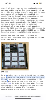
Does anyone have a digital copy of the IBM 5110 Logic Manual?

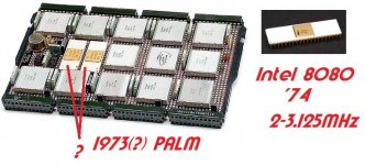
Or, any specific info about the PALM processor? For example, I see claims it ran at 1.9 MHz, but I don't see how that spec was determined.


At the following German site, between an IBM reference and referring to the old Linux 5110 emulator, some de-coding of the opcodes is available:
http://computermuseum.informatik.uni-stuttgart.de/dev/ibm_5110/technik/en/index.html
(they are trying to find the Chapter 2 of this reference)
 
I'm still not ready to pull cards out of my (working) 5110, but I do eventually want to get some higher resolution images of those.


Meanwhile, still just trying to understand the processing board. What are the 13 metal squares vs the two IC chips and is the metal-cylinder the crystal?

And I'm not sure how much the PALM changed from the 1973 SCAMP to the 1975 5100 release (and I'm assuming it didn't change at all in '78 5110 - other ROS cards did, but not the PALM itself?)


Just curiosities, no specific urgency.


cpu_note.jpg
 

Attachments

  • cpu_note.jpg
    cpu_note.jpg
    91.6 KB · Views: 5
The entire board is the processor. The square cans are gate arrays so collectively several of them do the arithmetic operations. I think it would take the logic manual and a lot of time following traces to figure out exactly what each can does and what the two ICs do. Something in that grouping is used to store the registers.

Chapter 3 of the maintenance manual has a high level overview of the components. The diagram includes reference to a clock being on the board so that should be a crystal.

Somewhere in this I found a reference to how the APL switch works. See page 3-18 of the maintenance manual. How to find the +APL switch line and tweak the Power On Reset function to do something different is beyond my level of knowledge.
 
I would guess but do not know that the two ICs could be ROMs containing the microcode --- in the sense of the word that's most commonly used today --- for the IBM PALM processor. Note that IBM also used the term "microcode" to refer to the System/370 and System/3 emulator software in ROS that ran the APL and BASIC interpreters. When I refer to the PALM's microcode, I mean it today's common meaning: data that orchestrates all of the the subsystems within a microprocessor in order to implement the instruction set.

I'm guessing you've included the 8080 chip image because, like these ICs on the PALM, it features a white ceramic housing. White ceramic for ICs seems to have been more common in the 1970s, so a number of chips could have looked this way even if they were not microprocessors. For example, I have a mid-80s Unix workstation that has an NEC hard drive controller in white ceramic.

That said, I think there may have been an 8080 in the IBM 5100 communications option card. I don't have this option fitted in my 5100, so I can't say for certain.

You might prefer to make use of the higher-resolution images here:
http://computermuseum.informatik.uni...onnectors.html
 
Update, I now have a physical copy of the "System Logic Manual" - it is a set of large fold out posters, which are difficult to scan. It is understandable why there is no digital copy so far.


BTW, of the three IBM 5110 processors I have, each of them has a different packaging of those "elongated" chips. The label on the black version is difficult to make out, but the other two are labeled:
2410085-C
LC 767620
7828 CT (in the middle version this number is 7907 CT)

The silver cylinder at the top (crystal?) is labeled 15.0917 MHz (not *the* clock rate of the processor, but perhaps some factor related to it). Typically "clock rate" is while cycles per seconds? So it would be both InstructionFetch and InstructionExecute ?

5110palm.jpg


As for the System Logic Manual, here is what the set looks like (with one of the posters unfolded)

I think they are all 4x2 pages. I suppose one could carefully cut the pages into individual sheets, then scan them that way. Alternatively, does anyone know of a facility with a post-sized scanner? Or I suppose I can attempt a quality overhead shot of each one (just a flatbed would be better to get shadows out from the creases).


IMG_1727_reduced.jpg
 
Last edited:
I "scanned" some blueprints recently by taping them (low stick adhesive tape) to a melamine board and photographed them with a 50 M pixel DSLR using a 90 mm tilt-shift lens for an effective dpi resolution of about 255. The results were reasonable, but the page folds made it hard sometimes to get nice images, and the low stick adhesive was a pain some times.
 
Oh wow. Please don't cut these up --- I suspect you can find some help in recovering good digital copies if you can't do this yourself.

One idea that comes to mind is getting a sheet of glass or perspex and flattening the unfolded sheets behind it before photographing them with an overhead camera. Glare would be a problem but should be something you can overcome with careful lighting.

I'd love to see anything like this for the 5100.
 
Just to follow up, in case anyone comes across this in the future... These were all scanned and are available here:


I mentioned this elsewhere, but didn't follow up here for completeness; and no, they weren't cut up :) However, now I'm not sure what to do with the original papers (which are folded, as they were originally). I read someone once stored a stack such as this in saran wrap, but that ended up collecting moisture (but perhaps after getting exposed to a flood - the wrap is still permeable). Should I store them just in regular cardboard, stacked? These can only be viewed by unfolding (they are posters). I'm happy with the digital copies, so do PM me if you can suggest a good physical home for this original set.

NOTE: The above link also has images of all the international character sets built into the display ROM, for lack of anywhere else to archive that.
 
I'm still not ready to pull cards out of my (working) 5110, but I do eventually want to get some higher resolution images of those.


Meanwhile, still just trying to understand the processing board. What are the 13 metal squares vs the two IC chips and is the metal-cylinder the crystal?

And I'm not sure how much the PALM changed from the 1973 SCAMP to the 1975 5100 release (and I'm assuming it didn't change at all in '78 5110 - other ROS cards did, but not the PALM itself?)


Just curiosities, no specific urgency.


View attachment 1224721
SIGNETICS N82S09I RAM 64x9 28-pin
 

Attachments

  • IMG_4119.png
    IMG_4119.png
    2.8 MB · Views: 7
I suggest a little fun for everyone - let's try to list all the ICs that the IBM 5100/5110 cards are made of - I was able to determine that "those two white 28 pin ICs" are SIGNETICS N82S09I RAM 64x9 28-pin - it seems to be a static memory RAM

ps. why can't I edit an earlier added post?
 
Back
Top