• Please review our updated Terms and Rules here

Original-IBM-5150 or IBM-Clone Memory Experimentation Thread

Ok, a preliminary check shows several pins on an LS08 (of which there are two near the memory, that control the RAS and CAS signals) not connected. This is just a preliminary, cursory check, though. I'll look at it more thoroughly later.
 
A further check with the logic probe shows that Pin 10 of one of the two LS08s has no pulse or HI-LO switching. The other one is functioning. Maybe that's my problem?

Pin 1 doesn't show HI-LO switching on either of them, but the pulse light does blink. Maybe the switching is so fast as to be unable to be shown with the HI-LO LEDs.

I'll check the pinout and try to connect the pins on a schematic page, using continuity mode on a multimeter, to see if it matches with any schematics I have. (There are 4 pins connected in-parallel to a refresh gate. Again, maybe that's my problem, that one is not connected?)
 
Last edited:
We can ignore the 24S10 PROM altogether.

So... I'm guessing now we move onto RAS and CAS?

… why can we “ignore the 24S10 PROM”? (And didn’t you say the machine didn’t even have a PROM like the 5160, but “equivalent“ discrete logic?) The purpose of the PROM in a 5160 *is* to orchestrate RAS/CAS generation/selection. If the A8 decoding is working that’s great, it means your memory banks in theory *should* be able to work, but if that decoding circuitry still thinks you have 256K total memory over four banks…

Do you have a schematic of what you believe at least is the equivalent to the 5160’s RAM address decoder?
 
I meant that we didn't have to get into the intricacies of the 24S10, if it came to it. (Like trying to figure out a black box) I'm going to be checking the RAS/CAS lines and the 138s nearby the RAM later today.

I happened to find this yesterday. Sorry, it's the closest thing I have. It may not be THE 775, but it's in the same system family. The 775 was not documented really at all...: http://www.eriscreations.com/sanyo/diskimages/sams-computerfacts-sanyo-mbc-55x-schematics-only.pdf
 
I meant that we didn't have to get into the intricacies of the 24S10, if it came to it. (Like trying to figure out a black box) I'm going to be checking the RAS/CAS lines and the 138s nearby the RAM later today.

What I'm not clear on at this point is if the 775 even *has* a 24S10? In the 5160 "intricacies" of the PROM are the whole heart of the matter; it's a piece of programmable logic that defines the possible RAM memory maps for the machine, and since it's the RAM memory map you're trying to change you need to know how it's set up on the 775 in order to know what to change.

Digging around the instructions for converting a "64-256K" 5160 to 640K it appears that from the start IBM programmed the PROM/PAL with both possible memory maps and it's whether pin 1 is connected to +5v or ground that chooses which mode it's in. The machine doesn't magically sniff out if you've added the multiplexer for A8 and installed larger chips, you need to *tell it* to use the alternate memory decoding. If the 775's stock memory decoder actually supports a 640K mode you need to find out how to turn it on. And if it doesn't use something like a PAL/PROM to hold both then there may be a component change necessary.

The schematics for the 550 are very unlikely to be useful; it's essentially an entirely different computer.
 
Last edited:
So, from what you're telling me, since the 24S10 is central to all this, in relation to the RAM decoding ICs (the 138s), I should be looking at the RAM ADDR SEL line, then.

(I'm looking at multiple schematics, at least 3, plus a university paper, just to make sure that there are enough similarities between all of them, to justify looking in that area. It seems feasible.)

Suddenly the logic contained in the PROM doesn't seem so complex... 🤔 On the clone schematics, I see LS00 chips in place of where the PROM would go. (The university paper tells me that there's a RAM decoding CIRCUIT, and a PROM Decoder [for those who managed to clone that too], which holds the logic for the memory map, in XT computers.)
 
Last edited:
Ok, looking over the other clone schematics, it seems I was hasty. Most of them used their own version of the PAL/24S10. Only ONE did not.

However... I've noticed something strange as I looked at my motherboard, when looking over all of the schematics, Pins 2 and 14 should be connected on ALL non-parity RAM chips! (That is, those that are not connected to the parity generator) Mine doesn't have that! I'm not sure if it would make a difference, but I'd like to try, at least.
 
Last edited:
However... I've noticed something strange as I looked at my motherboard. Pins 2 and 14 should be connected on ALL RAM chips! Mine doesn't have that! I'm not sure if it would make a difference, but I'd like to try, at least.

AAAAAGH! Do not do that. It will make no difference and depending on what's different about what Sanyo did you may well break something. Pins 2 and 14 are the "Data in" and "Data out" pins on that style of memory chip. If the Sanyo doesn't have them tied together across banks it might be doing something differently than the 515x, like using a separate data buffer per bank instead of one for all four. If the machine is working now it's working as intended, and this will have *absolutely no effect* on how memory is addressed. You'll just be shorting stuff together that for some reason Sanyo decided to separate, and possibly putting adverse loads on the non-enabled banks when the active one is trying to respond.

So, from what you're telling me, since the 24S10 is central to all this, in relation to the RAM decoding ICs (the 138s), I should be looking at the RAM ADDR SEL line, then.

YES. This is what I've been repeating for several posts, and I really tried to make it clear in this one, but let's try again.

An 8088 has 20 address lines, which all together can count in binary from zero to 2^20th, or a little over a million in decimal. IE, one megabyte. Your computer divides this possible total address space into chunks which are assigned to different functions, like RAM, ROM, video memory, whatever. All of these devices sit in parallel on the data bus, IE, the same data lines run to all of them, and they would all be shouting at the same time and stepping on each other if it wasn't for address decoder circuits to decide what was active and what wasn't depending on what address the CPU is asserting on the address bus.

RAM in a PC compatible starts at address HEX x00000h and runs in a contiguous block up to as high as x9FFFF. (640K) IE, out of the 16 possible 64K sections that fit in 1024K the first 10 are candidates to have RAM in them. Here is how a 256K IBM 5150, which does not have a PROM doing the job, sorts out how to assign each of four 64K banks of memory chips to one of four slots in the first 256K of the total address space:
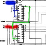
5150.jpg

A18 and A19, which are the top two address lines, highlighted in BLUE. With their 2 bits you can therefore choose one of four 256K slices of address space, which we will call pages zero through three. They connected to an LS138 multiplexer in such a way that the only used output line, which is "RAMADDRSEL" in this example, will be active low when "PAGE0" is active, IE, the CPU (or a DMA-driving peripheral) is looking to read or write the first 256K of address space, and inactive (high) all the rest of the time. This line, which I highlighted in GREEN, is used directly to drive the chip enable of a 74245 buffer that sits in front of all four banks of RAM, and it is *also* used as one of the enable lines for the LS138s that generate RAS/CAS signals; this is what gates ALL the RAM chips from trying to do read/write cycles when they're not being addressed.

Now look at the lines highlighted in RED. These directly connect A16 and A17 to the RAS/CAS multiplexers. A16/A17 again together give four possible selections, this time letting you choose one of four 64K blocks out of a total 256K range. The LS138s directly break that two bit number into the four RAS/CAS signals; since all RAM banks are the same size you don't need to do anything more elaborate than this, mapping directly to the address lines works. And that's basically it.

So let's see why the 5160 uses that PROM:
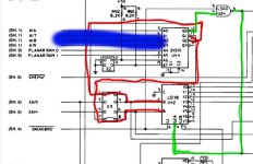
5160_decoder.jpg

On this system we have the 24S10 PROM in place of that 74LS138 in the 5150. This time the address lines, again highlighted in BLUE, which run to it include all four of A16-A19 instead of being split. The reason for this is because now we have the possibility of RAM banks being different sizes; instead of just being able to conveniently assign the same power-of-two granularity to all four banks you want two of them to be enabled according to this truth table:

A19A18A17A16Bank # (decimal)
00don't caredon't care0
01don't caredon't care1

IE, bank 0 needs to be active for all of the first 256K page and bank1 active for the second 256 page, while the other two need to follow this:

A19A18A17A16Bank # (decimal)
10002
10013

IE, when we're between 512K and 640K, A19-A17= 100, we want one of two 64K banks selected. In other words, we want an asymmetric equation to apply to what gets asserted on the RED lines which run to the CAS/RAS 138s. And, also, of course, we want that GREEN ADDRESEL line to be active when any of the banks are supposed to be active, IE, for the entirety of the bottom 640K block of RAM. To be clear, you don't NEED to use a PROM or PAL or whatever to do this; give me a few minutes to think about it and I could hack you together a schematic to do it with LS138's and some AND gates, or just NAND gates, or whatever, there's a million possibilities. The PAL/PROM just makes it easier because it means just one part can hold a bunch of different possible memory maps which can be switched between based on jumpers/switches.

(IE, look at the PROM in the 5160: it has eight address lines, of which only four are connected to the computer's address bus. The other four are connected to switches and jumpers. That means that the machine can support 16 different possible memory maps for RAM. This would be really messy and annoying to implement in discrete logic.)

That you're tossing out things like "maybe pins 2 and 14 on the RAM chips not being tied together" is the problem really makes me feel like you're not groking the basic concepts here.
 
My inability to latch onto information, and impatience, comes with the mental territory. (I'm autistic.) No disrespect was intended.

I didn't attach anything yet on the board.

I did, on the other hand, find something similar in a Turbo-XT manual (that allows for the same 640k capacity) on minuszerodegrees: http://minuszerodegrees.net/manuals/TurboXT - motherboard.pdf, that looks to have the same basic structure as what you posted. (I'm assuming the SA## lines here are equivalent to the A16-A19 lines to the PROM on the IBM schematic.)
TurboXT - motherboard (dragged).png


Here is where the SA16 line goes (I couldn't find the SA17 Line anywhere except for a connection to the BIOS ROMs and to an LS670, which goes right to the 8088). My system only has 4 LS138s like this schematic, and they are very close to the memory:TurboXT - motherboard (dragged) 3.png
And here is where those lines end up.
TurboXT - motherboard (dragged) 2.png

I'll check if my system matches this in some way or another.
 
Last edited:
Looking at the schematics for that generic XT, ugh, what a mess... but it certainly stands as an example of how to implement 640K decoding without a PROM. The decoding and CAS/RAS generation is very, very different from 5160. Tracing it is giving me a headache, but the long and short of it is the decoding section on page 6 appears to generate three selects, two of which (RAMSEL1 and 256/640SEL) are used to generate the CAS/RAS for banks 0 and 1 (which are the 256K banks), while the other select (RAMSEL2) is used directly with A16 to choose between the two 64K banks above 512K.

(Again, the schematics are a wreck, but if I'm reading them right essentially RAMSEL1 is active when the address is <512K, 256/640SEL is A18, and RAMSEL2 is active from 512K to 640K. RAMSEL, which is the equivalent of RAMADDRSEL in the IBM machines, is RAMSEL1 + RAMSEL2.)

Hopefully that helps you understand what you're seeing.
 
I seem to have been able to identify several similar component structures on my system where the PROM would normally exist (The RAMSEL page of the schematic), but there's also glue logic added in, and comparatively extraneous chips (when compared to a "chip-efficient" hacked-together system like the generic XT I showed you), which makes it difficult to figure out what to do.

I'm making some assumptions that I don't think are so bad:

Like before, I mentioned that the CPU address logic went off of the CPU/MEM board and onto the Video/ISA board that connects to it. However, the logic chips they stop at are very close to the ISA slots, and they have the same address lines as the memory, so I'm assuming those are meant for ISA interfacing.

Those same address logic pins also head in the direction of the 158s and 138s, so again, I'm assuming I would waste my time trying to figure those ISA address logic chips, and I should instead focus on the area with the 158s and 138s. (plus a 157 and 139)
 
Last edited:
FWIW, I found a photo of the MBC-775 logic board in a Google image search. The photo is of course far too small to be that useful (and the board is very crowded and possibly multilayered so I can't really follow traces anyway), but here's two observations:

1: I would wager the 74LS245 at U49 is the data buffer between all four RAM banks and the CPU data bus; this seems like a good guess because it's sitting right next to the socket for an unpopulated 74S280 parity generator, which would sit on the RAM-chip side of the buffer. The Sanyo's equivalent to RAMADDERSEL should be driving Pin 19 of this chip. Follow it and find out where it's coming from.

2: The empty socket for a 74S139 at U92 is very suspicious; if there is a "640K mode" that's present in the PCB but needs additional parts to enable a '139 could be part of that.
 
If you want, I have a larger photo of the board.

K5XKco8.jpg


I already populated the 139 footprint with a socket and IC. I also populated the parity generator socket just to make sure there was an extra layer of memory protection. (It's a weak layer, but still protection, nonetheless.) I'll take a look at U49 later.
 
Okay, you populated the '139, have you investigated what it's actually connected to? I see several open jumper positions in addition to a DIP switch, do any of those appear to relate to the memory addressing circuitry?

Remember, it's pretty unlikely this board has the ability to "auto-sense" which memory map you're using, just populating the parts isn't enough. Somewhere on this board something is going to have to be switched to utilize the alternate memory map, assuming it's actually functional.
 
The DIP switch is exactly in line with the 5160s, with the exact same settings. (It's how I was able to get EGA onto the system in the first place.) At its foundation (barring the memory decoding), this is a 5160 clone.

I did check the jumper on the lower left, and it seemed to be connected to the 139, but I haven't gotten a specific routing for that portion yet. I do have a complicated routing done for some of the chips, so I'll check that. I added a pin header to the J5 jumper footprint, but I don't know what that does yet either.

Edit: Amazingly, I DID figure out the routing for U49's Pin 19! It's connected to an LS02 NOR Gate at U11. (I'll recheck this to make sure, because somehow it doesn't seem right.)
 
Last edited:
So since they are the plumbing, I can ignore the 244s and 373s, can't I? I'll try to focus my efforts on the 139, 158s, 245s, and glue logic.
 
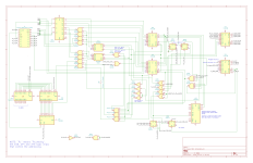
I'm not done yet, but I've taken a good stab at tracing out the schematic. I tried to keep it as clean and tidy as possible. I think the logic involved is worse than the Turbo XT I posted two weeks ago...

I'm ignoring the addressing logic (the "plumbing" that connects to the address lines), so if and when I reach them, I'll tack off the pin with a "To_373_PL"/"To_244_PL" label. (But if needed, I'll specify where it goes.)
 

Attachments

  • MEM ROUGH SCHEMATIC.png
    MEM ROUGH SCHEMATIC.png
    846.8 KB · Views: 8
Last edited:
Still not done, but I think one of the problems has presented itself in the schematic already:

Pins 9 and 10 may not be connected on U81, the LS08. The output of that goes to an Output Enable (Active HI) on one of the 245s. Pin 1, the DIRECTION pin on the 245, also doesn't seem to be connected either.
 
I was wrong. Pins 9 and 10 were connected just fine. I hope I have these connections correct. The logic on this looks messy. I had to assume that a few of the pins were disconnected because of the chips covering possible tracks. Finding one of the traces on U44 was too difficult, but I'll try to look for it if required.

I wasn't sure of where to stop, so I just kept going for a bit.

I also tried to clean it up as best as I could.

Like the note beside the 670 says, just let me know if I need to add more traces.
 

Attachments

  • Sanyo MBC-775 Mem Schematic.png
    Sanyo MBC-775 Mem Schematic.png
    371.6 KB · Views: 9
Okay, this is weird... I'm getting close to figuring out something...

JP5 on the schematic I posted, just for the sake of argument, may be the connection to this whole deal. (I may be grasping at straws here, though.) I just found a print ad with conclusive evidence that this system (and others by Sanyo) was meant to be expandable to 640k. :D

What doesn't make sense is that this jumper doesn't seem to do anything...
 

Attachments

  • sanyo print ad.jpeg
    sanyo print ad.jpeg
    170 KB · Views: 9
Back
Top