• Please review our updated Terms and Rules here

Automated backplane tracing tool

Vince, are you able to take a photo of the front and back of the entire backplane for me/us? :)
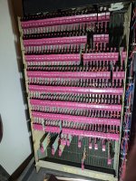
Well, I had to dig it out from behing the 8/I, but it was worth it, as I see now that I had double counted a couple of row when counting from the side. So it's just A-N.
PXL_20240707_204342588.jpg

I didn't uncover the front for a photo, but I did pull one cover and found that there's a ton of wiring on the four rows of slots. (Probably where all the cabling goes.)
 
Very cool, Vince. You certainly have a newer FPP12 with the big backplane!

I can't be sure, but I think the older FPP12 in the smaller backplane is the same as an FPP12-A. The backplane of the FPP12-A is prewired to support the FPP12-AE, which apparently adds EPM--extended precision mode. Haven't studied it enough yet to confirm for sure. I had previously assumed the FPP12-A was (by default) the extended precision variant, but it seems this may not be the case.

Just to think, all of an FPP12-AE would eventually be shrunk down to two hex-height cards a few years later!

Not to derail this too much with FPP discussions, but interestingly, the FPP8-A manual mentions that the FPP12-A is faster in all aspects other than load and store, in which the FPP8-A is "considerably faster." However, the FPP8-A can operate in "lockout mode," taking over complete control, rather than splitting time with the main processor. Thus, they claim in actual usage, the FPP8-A runs FORTRAN IV at about the same speed as the FPP12-A.
 
I'm not very fond of "too clever" approaches, and I feel like what I'm suggesting here might be one of them, fraught with potential problems related to programming. But, here goes...

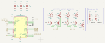
Here is the 8-bit unit, of which there are 9 per board.

Screenshot from 2024-07-07 20-59-52.png

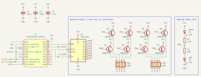
As I mentioned, rather disappointingly, the TSSOP-20 package of the Puya does not pin out PA9 and PA10 to offer a two-pin solution to the bidirectional UART lines. So, I found PA13 and PA14, which happen to also be SWDIO and SWDCLK, offer USART1_RX and TX, which can hopefully be connected to PF1 and PF0 without issue, and of course, to neighboring PA13/PF1 and PA14/PF0 pins.

Because I feel strongly about higher-current pull-ups, I found that JLCPCB (and LCSC) offers very cheap off-brand shift registers. But, for those that may want to build some boards for smaller backplanes or otherwise don't need the stronger pull-ups, these components are optional. Also optional (but recommended) would be the LEDs, which could signify software version at power-up or idle by means of a blinking pattern, or success/error conditions during a run. Note the ADDR0 and ADDR1 pins, which I'll discuss below.

I also am sticking with pins PA0 through PA7, which offer analog inputs. This may prove useful to measure the voltage on a net that is solely pulled high to see how much total leakage is present. It could give a rough indication of the total connections, or may give an indication that other components are on the net. Haven't exactly worked out all of the possibilities of this, but it seems worth investigating.

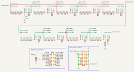
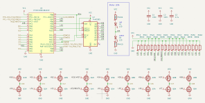
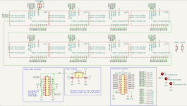
Finally, the entire schematic (minus the edge and expansion connectors; same as before).

Screenshot from 2024-07-07 21-40-01.png

The programming interface brings out all SWD pins, a common BOOT0, and completely separate nRST pins. I hope in this way, even conjoined SWD pins can still be used reliably if surrounding processors are held in reset. Any thoughts on this in particular? It's also possible that they can still be programmed via UART given these are also all TX/RX pins, but I don't know what the bootloader does with pin initialization. I could add cuttable solder jumpers in case I end up being wrong about my assumptions of tying SWD lines together--I would still have to have a larger programming interface, though. I also wonder if it's worth adding a 470 to 680 ohm resistor between pins in case one tries driving it high and the other low.

The ADDR0 and ADDR1 pins are optionally tied low to help determine where a microcontroller is relative to the left and right members on a board. This will allow for enough additional configuration to allow for identical addressing of the 72 pins no matter if the UART is flowing from left to right or right to left by passing the previously selected address to the next unit. This would also help detect any configuration issues since if (n mod 9) is 0 or 8, there should be a populated resistor.

I haven't tried laying this out yet, but would appreciate all of the feedback you can throw at it in the meantime.
 
  • Like
Reactions: cjs
According to JLCPCB, the PY32F002A is about $0.01 in the quantities we're talking about. That seems cheap--too cheap. Their source, LCSC, claims they are about $0.09 in the same quantity.

There is another Puya that is in a QFN-32 and allows for less sharing of lines, and would eliminate the shift register for controlling the higher-current pull-ups.

If JLCPCB's pricing for these microcontrollers is actually correct, I will plan to go with the QFN-32, which will make me more comfortable with the serial port situation. Even though it's 3.5x as expensive, it's the difference between $24 or so for 1,280 units, taking into account the added '164 with the TSSOP-20 design--all assuming JLCPCB's pricing. For whatever it's worth, JLCPCB's prices seem consistently ~7x less expensive than LCSC.

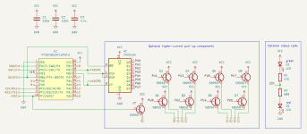
In any event, I have two designs for the now 9-bit units, which will shave off one more microcontroller per board:

Screenshot from 2024-07-08 18-51-18.png

The PY32F002A design is now relying on the fact that multiple people have confirmed the presence of two USARTs in the TSSOP-20, indicating it's probably the identical core as used in the bigger devices with the exception of flash and RAM sizes.

It seems nRST can be disabled and it's probably not strictly necessary for programming. Hence, it can be used to drive a ninth pull-up. There's nine total ADC inputs, with the ninth on PB1. The BOOT0 pin can be used after startup, so it now can control the reset for the '164, which isn't strictly necessary either, but why not.

And the QFN-32 design:

Screenshot from 2024-07-08 18-50-23.png

Now pins are dedicated, and there's also the possibility of using both UARTs in alternating directions, which I'm not sure adds any real value. I suppose if you are connected to both ends, you could set it up such that you only need to talk through n/2 total devices to get to the one you wish to address.

In both of these designs, since 9 is not divisible by 4, the resistor arrays are moved up in the hierarchy to take advantage of all resistors in the arrays without resorting to single resistors.

Really hoping to have a design finalized soon. I'd much rather be using them than designing at this point!
 
I believe you can connect the SWCLK and nRST pins on all the uC together and have separate SWDIO pins for each one. If memory serves the unused SWDIO pins should be pulled down, but it probably doesn't matter.

CW
 
It's been a while since I've provided an update. I've gone back and forth on a lot of details and have decided that higher current CMOS outputs would likely provide the best performance for the larger backplanes I'm trying to scan. However, the design is such that many of these components can simply not be populated if one wishes to have a smaller number of cards and rely on the internal pull-ups and weaker open-drain outputs.

Screenshot from 2024-07-19 11-12-13.png

I added external pull-ups and pull-downs to keep my mind at ease, such that the gates are always driven to a safe value if they are not being directly driven by their respective drivers.

Screenshot from 2024-07-19 11-16-18.png

Thinking about how long one message would take to traverse every single microcontroller, even at reasonably fast baud rates, I decided that it would make more sense to have exactly one microcontroller on every board act as a master, and each master talks to a loop of 7 microcontrollers. The same code can still run on all microcontrollers, as any microcontroller that detects a resistor on the ADDR line will configure itself as a master, or otherwise, as one of seven in the smaller loop.

Because SWDIO and SWDCLK are not repurposed, I shouldn't actually need nRST or BOOT0. In fact, I shouldn't need BOOT0 at all if I don't wish to use the internal serial bootloader, which would likely not be used. But, those are pinned out just in case to some surface mount pads on the backside.

VDD connects to all of the PFETs and will be fed with some constant current source from the main controller board. This way, you can select the constant current limit and more accurate measure resistances between two pins. If the analog voltage read is too close to zero, the current can be stepped up until it is above some satisfactory threshold, or the maximum current (to be defined by the backplane under test) has been reached. The MOSFETs are good for 2A, but I was thinking 500 mA max or so. This backplane tester would hopefully then be able to determine any pins that have higher resistance and might require attention.

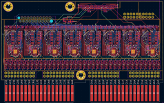
The layout has proved rather challenging, but it's coming along.

Screenshot from 2024-07-19 11-20-24.png

The programming header is a Würth part that seems pretty well suited for quick connection without requiring a mating connector: https://www.digikey.com/en/products/detail/würth-elektronik/490107672012/7917224

I hope in the next week or so, I will be able to order a handful for testing before making a big order.
 
Nice layout! Dense and systematic.

… have decided that higher current CMOS outputs would likely provide the best performance for the larger backplanes I'm trying to scan. However, the design is such that many of these components can simply not be populated if one wishes to have a smaller number of cards and rely on the internal pull-ups and weaker open-drain outputs.
Seems like a good option to have and easy to configure either way.

What’s the manufacturer part number or JLCPCB/LCSC “C”-number of the dual transistor?

Transistor can connect VDD to pins of the microcontroller which is powered by VCC. Is VCC and VDD the same back at the source/main board?
 
Nice layout! Dense and systematic.
Thank you! I thought I would have to go to two-sided assembly for sure, but what do you know! It fits on one side with some room to spare.

What’s the manufacturer part number or JLCPCB/LCSC “C”-number of the dual transistor?
It's a knockoff of the Si1553CDL from Vishay: https://www.lcsc.com/datasheet/lcsc_datasheet_2305051409_VBsemi-Elec-Si1553CDL-T1-GE3-VB_C558238.pdf

Is VCC and VDD the same back at the source/main board?
VCC is generated from an on-board 5V regulator fed from VIN, which I anticipate being 6 to 12V. I thought about using a low-cost switcher instead of a linear regulator and may still do so, but a linear always seems easier. I don't actually have a good gauge on how much power each board will use yet. I think that's pretty heavily dependent on programming, sleep mode, etc.

VDD is a current source, yet to be designed. It will probably end up being a 5V supply fed through selectable resistors, spanning a few decades, from 10 ohms to 100k ohms.

You might consider something like this for the programming connector.
I like that, but in the event that I need to program these when stuck in a backplane, I think I can probably squeeze the other connector into position, though it might be a hair too tall. I dread the thought of having to program the boards a second (third, fourth...) time. It may be worth trying to write a software update routine that works through the daisy-chain. That would be nice.
 
Suddenly, I had an idea that if I were to successfully reproduce PDP-11/70, I would provide an accurate list of backplane connections that could serve as a test pattern.
By checking each connection one by one according to this list, We could determine if all connections were correct
This way, the coverage rate can be 100%
The 11/70 backplane got up to revision T. Revisions L and later have an etch that replaces critical signals carried on regular yellow wire (and a ground pin in the etch) to a twisted pair of black and white wire. So, even if you create a complete list of interconnects, you'll still be missing which ones need to be routed specially or done with twisted pair.

There are also a bunch of signals that go from one board to another, something gets done, and the signals come back to the first board. That's just because the necessary components overflowed the available board space, given early 1970's design constraints. Stuff got shipped off to free space on another board, then comes back without it being used for anything else on the other board, just because the other board had free space.

Consider the never-marketed KE74 CIS option for the 11/74 (the 11/70 + CIS, not the 11/70-MP that got renamed to the 11/74 when the CIS option was stopped). I believe the plan was to double the capacity of the existing microcode ROMs, keeping essentially the same microcode (aside from dispatching the CIS instructions) but adding some or all of the CIS microcode. I don't know if that was for the "simple" CIS instructions that would be handled by the existing 11/70 CPU, assist for dispatching to the KE74, or the entire KE74 control store (I doubt that, given the complexity of the control store on the KE44). In any event, with one of the Massbus slots re-purposed for holding the CIS board set, that would have been a lot of new, long signal cables between the Massbus slot and the control store area of the CPU.

In any event, "re-creating" the 11/70 CPU is sort of the same dilemma VSI faced when initially announcing their intent to port VMS to the x86-64 architecture. I asked if the goal was:

1) To preserve feature, syntax and bug compatibility with earlier VMS systems (essential for customers who wanted to get off Itanium or Alpha VMS with a minimum of fuss, and hopefully avoiding recompilation)

2) Implement modern compilers to attract customers new to VMS (essential, because they want to take their Linux/whatever code and run it on VMS to take advantages of features like clustering without re-writing into ancient language dialects). As someone who tried building Perl on VAX/VMS, I can tell you it is not simply "./configure; make" as it is on Linux.

3) Some combination of the two, since the installed base is by definition a shrinking market. How fast it is shrinking is unknown, probably even to VSI, because their only view into it is how many support contracts they'd sold for Alpha and Itanium VMS.

Those are three mostly-incompatible goals (#3 requires a C compiler that accepts both "/STANDARD=VAXC" and also the latest c++ extensions, or maintaining two separate compilers, with the same being true for Fortran and Cobol, at least. I'm unsure of the issues with Pascal, and DEC-ish BASIC is pretty much unique to VMS).

Getting back to your 11/70, we can assume that the goals are:

1) Talk to the original front panel or a faithful replica
2) Execute the original microcode faithfully
3) Support (some subset of) real 11/70 periplerals
4) Allow execution at both "real 11/70" speed as well as a "turbo" speed of whatever the new hardware can run reliably at
5) (Maybe) Add CIS and the 11/93 TOY clock as well as memory battery backup
You can do that by re-creating the original boards and backplane (a huge amount of work), implement the same logic using modern components (possibly with physically smaller boards w/ SMD components, a smaller number of boards, or both). Let's face it almost none of the people who "want" an 11.70 have either the space for it or the desire to pay the power bill for running it. Look at how successful the PiDP-11 has been, even though it is a miniature front panel with a Raspberry Pi running simh behind it. SO you're going to have to miniatureize it somehow.
 
The 11/70 backplane got up to revision T. Revisions L and later have an etch that replaces critical signals carried on regular yellow wire (and a ground pin in the etch) to a twisted pair of black and white wire. So, even if you create a complete list of interconnects, you'll still be missing which ones need to be routed specially or done with twisted pair.

There are also a bunch of signals that go from one board to another, something gets done, and the signals come back to the first board. That's just because the necessary components overflowed the available board space, given early 1970's design constraints. Stuff got shipped off to free space on another board, then comes back without it being used for anything else on the other board, just because the other board had free space.
Ah. That helps explain the *amazing* number of twisted pairs on the backplane. I had assumed that they were mostly TIG-related, but this "shipping critical path signals" round-tripping would likely be a big user of those.
Consider the never-marketed KE74 CIS option for the 11/74 (the 11/70 + CIS, not the 11/70-MP that got renamed to the 11/74 when the CIS option was stopped). I believe the plan was to double the capacity of the existing microcode ROMs, keeping essentially the same microcode (aside from dispatching the CIS instructions) but adding some or all of the CIS microcode. I don't know if that was for the "simple" CIS instructions that would be handled by the existing 11/70 CPU, assist for dispatching to the KE74, or the entire KE74 control store (I doubt that, given the complexity of the control store on the KE44). In any event, with one of the Massbus slots re-purposed for holding the CIS board set, that would have been a lot of new, long signal cables between the Massbus slot and the control store area of the CPU.
Didn't know where they were thinking of fitting in the CIS. And the first Massbus controller is basically at the opposite end of the module-set from the primary CPU control, so long(ish) wires.

I was thinking that they might have considered moving the existing module-set X positions to the rear so as to enable X new module positions between the first module position (M9301 Unibus terminator, KW11, KM11) and the FP11 module-set. That would greatly reduce wiring runs and put the CIS modules fairly near the FP ROM and ROM Control (M8128).
Getting back to your 11/70, we can assume that the goals are:
...
5) (Maybe) Add CIS and the 11/93 TOY clock as well as memory battery backup
AFAIK one would have to create CIS microcode from scratch, right? The 11/44 CIS microcode would be a useful "algorithmic/design" reference, but that's about it AFAICS.
 
Please use the other thread to discuss 11/70 topics.

I've been trying to get prototypes ordered, but the Si1553 dual MOSFET that I picked has been quoted at almost 6x the price advertised on LCSC by JLCPCB... I may have to redesign with individual NFETs and PFETs to make the run substantially more economical.
 
I've been trying to get prototypes ordered, but the Si1553 dual MOSFET that I picked has been quoted at almost 6x the price advertised on LCSC by JLCPCB... I may have to redesign with individual NFETs and PFETs to make the run substantially more economical.
It might be easier to find a cost-effective and electrically compatible solution with individual P and N MOSFETs. The problem is the two parts would be larger than the Si1553. It would be probably easier to find alternate parts later if you use separate parts, in case the dual MOSFET is out of stock. I see now that there are only qty=15 in stock
 
...

Didn't know where they were thinking of fitting in the CIS. And the first Massbus controller is basically at the opposite end of the module-set from the primary CPU control, so long(ish) wires.

I was thinking that they might have considered moving the existing module-set X positions to the rear so as to enable X new module positions between the first module position (M9301 Unibus terminator, KW11, KM11) and the FP11 module-set. That would greatly reduce wiring runs and put the CIS modules fairly near the FP ROM and ROM Control (M8128).

...

The CIS option in the 11/74 occupied the first four slots in the 11/74 backplane.
The whole CPU section was shoved down by four slots to make room.
Because of that, one RH11 controller complex was eliminated from the revised backplane.
 
I haven't worked through the details, but it would be nice if you could pull a pin low through a known resistor (1% perhaps), measure the voltage, then release it and allow a remote card to pull the pin low through the same size resistor. You should be able to maths the resistance of the interconnect wire to determine if there is a corroded connection. Probably best in a post-processing step once the netlist is determined and not during the initial scan.

CW
 
That's exactly what my current design will let you do, and the reason it's multiplied the cost more than I had hoped! The resistor(s) sit on the driver board and will feed all of the PFETs, of which only one will be on at a time. Hence, you should be able to get a decently accurate resistance measurement depending on the resistor chosen. That said, it will not be able to perform a 4-wire measurement, so there will be error.
 
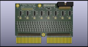
I submitted the first prototype run of 10 pieces of the paddle card to JLCPCB for assembly. I decided the pull-up and pull-down resistors for each MOSFET gate were probably ultimately unnecessary, so they disappeared.

backplane_tracer_v5_front.jpg

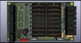
I also submitted my driver board:

backplane_tracer_driver.jpg

The left four relays are for controlling an optional red, yellow, and green LED tower (obviously optional) with an external buzzer/beeper. For something that may be running for hours upon hours, I figure one may want to be notified in the event of a failure or success.

The Teensy 4.1 has 8 serial ports, and I am using some level shifters with enables (TXU0204) to effectively give 16 serial ports, of which only 8 would be active at a time. This is an attempt to reduce the latency associated with very long daisy-chains; they can instead be broken up into smaller chains.

12V is supplied via the bottom connector (no 3D model, but it's supposed to be a screw terminal, along with the left relay outputs).

The relays on the right, along with some 1% resistors, provide different current limits for testing, in hopes to allow for a more accurate resistance measurement if that is so desired. There's a few op-amps on board to also measure the test current. I thought about adding a current sensor for the main 12V power rail fed to the paddle cards, but I opted against it due to real estate and time.

Anyways, there's quite a bit of software ahead now! Any volunteers? :)
 
Back
Top