• Please review our updated Terms and Rules here

Commodore PET 2001-N garbled and truncated screen.

me96jvb

New Member
Joined
Feb 19, 2024
Messages
4
Hello,

A few months ago we bought a Commodore PET 2001-N in a known-to-be-not-working condition. It had, apparently, spent the last 30 years of it's life hiding in a loft and copious dust and rust bears that out. I have fixed several problems so far (see the end of this post, in case it is relevant), but I have 3 problems that I cannot solve. For the first problem, I think that I have come to the point of having to test the CPU, RAM and ROM but I want to make sure I haven't missed anything else first.

The 3 symptoms:
1. Garbled screen (see picture)
2. The display goes to black after about 3 minutes. It recovers after being switched off for a few minutes, so I'm suspecting a thermal problem.
3. The display is slightly truncated at the top. (See picture). It is completely alleviated by reducing brightness to minimum.

My observations:
-The +5V, -5V and +12V regulated rails are all within 2% of what is expected.
-All 6332 ROMs at D6-D9 and F10 have about 4.9V at pins 21+24, and all are quite hot to the touch (although D7 is notably cooler).
-All RAMs (now) have -5.1V and are all cold to the touch.
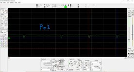
-The 555 reset output (Pin 2) toggles Low - High - Low at switch on.
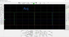
-The CPU reset Pin 40 is held low for about 1 second at switch on (Pin 40 goes: Low -> High, not High -> Low - > High)
-The CPU is warm to touch


Is the behaviour at CPU Pin 40 correct? Or should it be High -> Low - > High?


I have a logic probe and oscilloscope and a basic knowledge of electronics (although that last point depends on your benchmark, I suppose).


Here is a brief my-PET history, in case it turns out to be relevant:

I have found and repaired these problems so far:
1. The -5V rail was unstable and reducing to -7V (>>> replaced VR6 and then Diode CR13)
2. There was no vertical sync (single horizontal white line) (>>> replaced G10 and H10).
3. There was originally 0V at ROM D7 and D8. (>>> reseated chips)
4. Repaired cut track (INIT line to H1 Pin 12)

I have also replaced Capacitor C62, as I had one.


I suppose the first thing is to ask whether the CPU reset pin behaviour is as expected...?

Thanks

Justin
(UK, Norfolk)


IMG_1278.jpegIMG_1107.jpegIMG_1279b.jpg
 
Last edited:
Welcome to VCFED Justin.

I will answer your questions a bit later once I have woken up and checked the schematics...

Dave
 
The CPU reset line is active LOW. So as long as it is low for about 0.5 to 1.0 seconds at power-up, then goes HIGH you should be good.

At the moment of power on you may have the odd strange effect occurring.

The garbled screen usually (but not always) means the CPU has given up executing instructions. Check pin 7 of the CPU (SYNC) for a pulse. You get a pulse on this pin every time the 6502 CPU executes an instruction. No pulse, no instructions...

How to proceede from this point...

The usual way would be to construct a NOP generator and use an oscilloscope to check the address lines and address decoding first. Then download a copy of my PETTESTER and burn it into a 2K EPROM to replace the EDIT ROM.

Alternatively, you can buy a ROMulator that is inserted into the CPU socket containing ROM and RAM replacements (including TEST ROMs) and including a NOP generator.

Yes, the screen going black could be an indication of overheating. I would check to see if the voltage regulator in the monitor is getting too hot and shutting down as a result. It may just require the old thermal paste between the regulator and the heatsink renewing.

That case has definitely got measles hasn't it!

Dave
 
Last edited:
There was an interesting problem found in a 9" PET VDU, it was thermal.

There is a 7812 voltage regulator attached to a large heat sink in the VDU. They pushed it about as hard as they could from the thermal perspective.

Some VDU's, they used a rivet to attach the regulator heat flag to the heat sink. The rivet distorts the heat flag, and over the years, the white thermal paste dries out and goes powdery reducing the thermal coupling between the heat flag and the heat sink. The regulator then overheats, initiating thermal shut down a while after the VDU is powered. To find out if this is the case use a temp probe with a small bead and measure the heat flag temperature, vs the black heat sink nearby.

If this is the case, replace the rivet with screw/nut/washers and apply fresh heatsink compound.

Other monitor issues include bad soldering to the pcb where the connector pins for the plug fit, and 360 degree ring fractures in that soldering.

Of course, the image can disappear from the VDU, when the VDU is ok, if the H drive pulses go missing, that will kill the display, as will the video signal from the main board going missing.

You PET is the Dynamic PET board. These are usually fairly easy to get working. Many of them tend have at least one or two of the video SRAM chips defective and the occasional defective DRAM IC.

Most people start with a NOP Generator to check out the hardware , and then the PET Tester.

If you look at the capacitors on the power supply filtering areas, next to the DRAM IC array, you will see these are green bead Tant types. Many of Commodore's Dynamic pcb's used yellow jacket electrolytic caps, that are invariably ok. But, this is not the case with the bead Tant types that have a penchant for going short circuit. So it is worth checking the power supply rails there in the DRAM area.
 
Last edited:
Thanks Dave and Hugo,

Yes, both +5v rails are good.

I have a SYNC pulse on CPU (pin 7). 142 kHz.

Hugo was spot on with the 360deg solder fracture! I found 2: one at the VDU connector pin 9, and one at a capacitor (can’t recall which one). I reflowed the joints, and the VDU has stayed on for 2 hours. I decided to leave the heat sink alone for now, but will add a couple of aluminium “radiators” at some point.

As one of the reasons for this project is to improve my skills and understanding, I think I’ll make a NOP generator before moving on to a ROMulator device if required.

So, if I understand my research, I think I need to get 0xEA onto the data lines of a sacrificial CPU, which would be:

Pin
33 0
32 1
31 0
30 1
29 0
28 1
27 1
26 1

Right?

What I can’t quite fathom out is what to measure. Am I going to measure the pulse frequency on each pin of the address bus?


Justin
 
Last edited:
Excellent work on identifying solder fracture.

Yes, you are spot on about your sacrificial CPU. Bend the data lines out (pins 26 through 33) and strap them as you have identified.

The first thing is to use your oscilloscope and check all of the address lines for the correct frequency and 'sensible' looking TTL levels.

A0 should be 250 kHz, A1 should be half this frequency (125 kHz). Each subsequent address line should be half the frequency of the previous one.

After that, check all the address lines at the pins of the components where they are supposed to go to (following the schematics). This checks the address buffers, the PCB tracks and the IC socket connections.

After you have done that, we can check the address decoding logic through to see that the various sub-systems are being addressed correctly.

If you have a scrambled screen, but the CPU has a signal on the SYNC pin (pin 7), this could be an indication that the address decoding logic is not working correctly for the screen. However, this is a guess on my part - but we should 'work the problem through'.

Dave
 
I would (quickly) check the following:

1. Install a normally-open pushbutton across capacitor C68 (0.1 uF). The capacitor is connected between 0V and pin 2 of the LM555 timer (A2). This button forces a manual reset when pushed and avoids the constant turning OFF and ON of the PET when diagnosing problems involving a RESET condition, or just after a RESET condition.

2. Check F6 pin 1. You should observe a 1 MHz clock.

3. Immediately after a manual reset, check for activity on F1 pin 6. This signal should normally be LOW and have a burst of activity after a reset as the screen is cleared. Following a reset, there may also be further activity on this signal.

4. As above but for A5 pin 12. This signal should normally be HIGH with low-going activity.

5. As above but for A6 pin 7. This signal should normally be HIGH with low-going activity.

Dave
 
Thanks Dave,

I'm waiting for a part for the NOP generator.

I installed a normally open momentary switch across C68 + and connector J3 Pin A-1 which is conveniently nearby.
It was simple enough and I have no regrets doing it, but since installation, I've noticed a change in behaviour.

The main thing is that I cannot get a reset on Pin 40 (stays high) and a permanent Low on CPU Pin 7 (previously pulsing).

I double checked my switch installation and it seemed fine, nevertheless I've removed it to recheck a few things.
Before fitting the switch, I had been cleaning the board in that corner with IPA; its possible that I inadvertently damaged something. Lesson learned: leave engrained dust alone, and re-check functionality before making an alteration.

Without the reset switch, on power up, I have:
A2 Pin 3 High -> Low (good)
A3 Pin 1 High-> Low (good)
A3 Pin 2 Permanent High (bad)

I also notice that the voltage across C68 is tending to 2.1v (which is above the threshold for 555 timer, fine, but I was expected it to rise to 5V).

To allow further checks - Do you think its reasonable to trigger a reset by momentarily grounding A10 Pin13?


Justin
 
Last edited:
I would check the voltage directly across pins 7 and 14 of A3 (74LS04).

If that is correct, just check that the logic input voltage on A3 pin 1 is going below 0.8V (a true logic '0').

If so, it is likely that A3 has gone faulty (or some PCB track is damaged somewhere).

Before replacing A3, you could also check the other gates within the A3 package to see whether anything else is affected.

If you notice, /RESET is wired to connector J4 pin 22. So you can ground this pin if you wish. A10 is an open collector gate, so is perfectly safe to 'wire-OR' this signal to 0V. This is also pin 40 of the CPU.

Dave
 
Thanks Dave,

I installed a CPU reset a switch across C68 and made a NOP generator. (I made the NOP generator using a second socket between the CPU and the board).

Some progress to report, but I'll split it into 2 parts.

1. CPU reset
2. CPU addressing


1. CPU Reset.

As I mentioned in a previous post, I've been chasing a confusing and intermittent CPU reset problem. Initially it seemed that there was a problem with A3 (74LS04) but, cutting a long story short, it turns out that actually the problem is that A2 (555) Pin 3 does not always get pulled low after a reset. Initially I did many of my checks of this problem with just a DVM and this lead me down a dark rabbit hole. With the DVM, I thought that I was measuring 2.5V across C67 (>3.3V is needed). This made me suspect and replace C67 (and I replaced C68 too because I was in the area). Replacing the caps did not fix the problem. I checked R15 (OK) and R16 (OK). Then replaced the 555 chip but did not fix the problem. It was only at this point that I checked using an oscilloscope and I realised that what I thought was 2.5V across C67 was actually some average/RMS value. In fact, C67 is charging to 3.3V and then Pin 3 gets briefly pulled low, but then Pin 2 seems to get pulled below 1.6V and I think this causes the sequence to reset and repeat. (Pictures attached).

555 Reset repeats at about 1Hz, sometimes for several minutes. Eventually the system stabilises at the expected positions.
It seems to improve with temperature (I think) and after around 15 minutes of being on, resetting becomes reliable.
Its something I will take into account while carrying on.

2. CPU addressing

After ensuring that a reset had occurred, I checked the items daver2 suggested:

F6 (Pin 1) - 1 MHz
F1 (Pin 6) - Is normally Low. No activity after a reset.
A5 (Pin 12) - Is normally High. No activity after a reset.
A6 (Pin 7) - A6 isn't populated.

I made NOP Generator. The address lines are not pulsing, and some have intermediate (floating?) voltages.
Voltages on the Ax pins listed below, with some other relevant pins. Measured with a 'scope.

Pin 40: High (4.85V)
Pin 7: 500 kHz
Pin 26: 4.8
Pin 27: 4.8
Pin 28: 4.8
Pin 29: 0
Pin 30: 4.8
Pin 31: 0
Pin 32: 4.8
Pin 33: 0

A0: 0
A1: 0
A2: 0
A3: 3.3
A4: 0
A5: 1.1
A6: 0.5
A7: 0.6
A8: 1.3
A9: 1.4
A10: 1.4
A11: 1.4
A12: 1.4
A13: 2.0
A14: 2.3
A15: 0
 

Attachments

  • A2_555_Pin2 to Gnd_cont resetting.JPG
    A2_555_Pin2 to Gnd_cont resetting.JPG
    258.2 KB · Views: 6
  • A2_555_Pin3 to Gnd_cont resetting.JPG
    A2_555_Pin3 to Gnd_cont resetting.JPG
    272.2 KB · Views: 6
  • A2_R15_5v side to Gnd_cont resetting.JPG
    A2_R15_5v side to Gnd_cont resetting.JPG
    254.8 KB · Views: 6
I am now a little confused about which machine we actually have. Can you identify the Commodore assembly number of the PCB please.

Your 555 issue smacks a little bit of a really horrid fault we had a few years ago. I suspected it was left over flux (or something similar) causing short circuits. The 555 was removed and the PCB cleaned (top and bottom) and the problem went away. This was after replacing every component in sight in the reset circuit...

Let's ignore the NOP generator until we get the RESET working correctly.

It doesn't really make sense to have the address pins like that...

Dave
 
With regards to the 555 timer circuit (apart from the output on pin 3) if you are making any measurements of it, they have to be done with a x 10 scope probe, the reason is that it is a high Z circuit with 1 Meg charging resistors.

The idea of it is, a one shot. When the power is initially applied, both C67 and C68 are in a discharged state. Therefore the trigger pin 2 in low initially, this triggers the IC so that its output pin 3 goes high. It stays in this state until C67 charges up to to the threshold voltage (which is 2/3 of the 5V supply) a second or so later. However for the 555 to give the 1 second high output on pin 3, it is very important that the low trigger voltage has gone high again, before the 1 second time set by C67 (1uf) and the 1M charging resistance terminates the the high pulse out of pin 3.

Now the trigger voltage pulse, in theory at least should be short, because the value for the capacitor on pin 2 was chosen at 0.1uF, the time constant is only 100mS and a lot shorter than the timing period of about 1 second.

The first thing to check therefore is if the resistors capacitors are the correct values and there is no mix up between C67 and C68.

It could be possible, that if there is leakage on the pcb surface (leaked capacitor electrolyte can do it or possibly flux, because it is a high Z circuit) that the when the threshold voltage is reached and the discharge deployed to discharge C67, that this low going transient is being passed to the trigger input pin 2 via a leakage pathway. That would then turn the circuit into an Astable (oscillator) with about a one second period high on pin 3 and a narrow low pulse in between. Any amount of leakage, if it was in fact there, would have more of an effect doing this, if the value of C68 (0.1uf) was too low, say if it was accidentally a 0.01uF and not a 0.1 by mistake. So it is important to double check the capacitor values.

It could well be the same issue as Daver2 mentioned happened in another PET.
 
Back
Top