• Please review our updated Terms and Rules here

CPD1604S Vertical Collapse

vol.2

Experienced Member
Joined
Dec 4, 2018
Messages
276
Location
baltimore
So I got this Sony PC monitor from 1992 that didn't work when I picked it up. I went ahead and tested all the caps and replaced anything bad. There was a absolute ton of caps that had gone high ESR (we are talking 300kOhms high) and there is one board in particular, the DA board, that used surface mount caps which had leaked all over the place.

On the DA board, I removed all the caps and clean it thoroughly with white vinegar and let it sit until it stopped foaming. I cleaned that off and then soaked it with 99% IPA and dried it off with compressed air and let it sit for days to make sure it was dry. The DA board is almost all surface mount, and there are no transformers or anything that might get messed up by being wet. I sprayed all the pots with deoxit and fiddled them a bit to make sure they didn't harbor salts or crust from the whole process.

I also inspected the DA board under a microscope and tested continuity on any areas that seemed more corroded. There didn't appear to be any such issues, and the traces didn't seem to be broken, only exposed in some areas. I suppose it's possible that something under an IC is bad, or a via got damaged because it's a multi-layered board with components on the back side. There is absolutely no apparent damage to the back side.

When I got everything back together, I turned on and I got HV, but the image was vertically collapsed. It's only a few pixels high, but it's there enough that I can actually make out the colors in the line and it reflects what should be seen on the screen. For example, I can see where the Windows logo starts and stops on boot, and I can see the proper colors change on the raster horizontally (for example a SMPTE bar image will reflect the bars color across the screen). I can also successfully shift the image horizontally with the screen controls.

My first thought was that the bad caps on the D board might have blown the Vertical Output IC before I got it, as I have run into that issue a number of times. I bought a handful of the ICs pretty cheaply, but replacing it didn't help or apparently change anything. I thought maybe the replacement could be bad, but a thorough check of the original IC revealed no shorts on the IC, and diode tests between pins seem to make sense for a working IC. I don't believe the original IC was bad at all. I suppose it's still not impossible, but I think it's okay. Anytime this has happened to me in the past, the IC had shorts or low resistance between GND and Vcc or some other pin(s).

So I'm kind of lost here just checking random things. It's extremely difficult to test voltages on this monitor because the portion of the case that holds the CRT is extremely thin and can't be supported by it's structure alone. The only way I could get it to stand up and make adjustments on the inside was to prop it up leaning forward on a towel and balance it that way. Doing this it's not possible to access the bottom of the PCB to take readings. So I disassembled the chassis again and I'm just looking more closely at the DA board in hopes that I can find a culprit.

There are a number of small ICs on the DA board that handle all the V and H stuff, and choosing the resolution, I assume based on the frequency of the incoming signal.

Can someone help me to identify which components or areas can cause this condition? Again this is:

-General Vertical Collapse

-There are still a couple of pixels present, enough to match what you are displaying to those few lines as the input changes

-Horizontal seems to be okay in that it spans the whole screen and it is movable with controls

-High Voltage appears to be present as I'm getting the whine and the static on the screen

-Area around the Vertical output IC on the PCB is dark from heat, but none of the component are visually burned or bad and testing a couple so far they looked perfect.

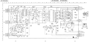
Here is a link to the three pages of the schematic on imgur. I didn't want to put them in-line as they are 11x17 size and would be too big here. If you open the image links and then view them in another tab, you can expand them to see details.

D board:
DA board:
Neck board:
TIA
 
Last edited:
I was able to get the thing balanced in a way I could take some readings with my scope, and I can at least confirm that I'm getting the correct Vertical deflection signal on the output of the DA board, so maybe this indeed about the Vertical not spinning up on the D board.

I'm not sure what to check next. I replaced the Vert output IC (and also tested the old one a bit and it basically looks okay), and I replaced any bad caps on the board, which included everything surrounding the Vertical IC anyways.

I double checked the orientation of caps and I went over the entire Vertical section and reflowed the solder. Nothing looks visually bad.

Maybe there's some kind of protection diode or a bad relay or something? I can hear a relay click on the board when I insert a VGA signal, but it could be bad in theory.
 
Some things you did though were a bad idea. If a pcb is contaminated with an ionic substance such as the electrolye from leaked surface mount caps, the last thing you want to do is to add more ionic contamination such as weak acids. Also, cleaners like IPA won't work either. The only treatment method which works is to leach the electrolye out over time, preferably by running warm deionised water over the affected area from a water stream set up over a sink to do it, tap water is better than nothing, but if that it used it still needs a final wash with deionized water to remove the residual salts in the tap water. Do it, ideally for a couple of hours or more. It takes time. The board can be cleaned later with IPA if wanted and warm air dried but the conductive ions must be removed first. People have suggested on the internet to use substances like vinegar to clean affected pcb's and other parts, but frankly, they haven't go a clue what they are doing and only making matters worse. Also foaming effects applying weak acids (which seem to delight people) are no guarantee of resulting compounds that won't be electrically conductive or have a neutral PH.

Also global replacement of caps can be a risky proposition, especially if a fault is introduced along the way. Still if you have done that properly with the correct parts, its one less issue to worry about.

You said:

The DA board is almost all surface mount, and there are no transformers or anything that might get messed up by being wet.

This could not be further from the truth. One of the most common parts to fail on a surface mount board after being in contact with leaked electrolyte (typically from a surface mount electrolytic, notorious for this) is the surface mount resistor (of which there are many). The electrolyte eats away the film in the resistor, typically they go O/C. Also a couple of other things that get damaged are thin copper pcb tracks that hide under surface mount IC's, where electrolyte collects, these can be eaten right through, and also plated trough holes can be rendered open circuit. Often its possible to see which of the surface mount parts have been in contact with electrolyte because the solder loses its sheen, acquires a dull grey look and the surface also becomes both a thermal and electrical insulator typical of oxides.

Generally to make sure the board is ok it requires the deionised water treatment, checking the continuity of tracks, especially ones that go under IC's and routed via plated through holes and checking an replacing any affected surface mount parts. Its a big job. And you only have to miss one defect for the board not to work.

Back to the failed Vertical deflection. If you have a vertical deflection IC that is not putting out drive to the yoke, the first move is to look up the IC manufacturers's application note. Then test the IC pins one by one with a meter and a scope. In most cases it becomes clear from doing that why its not working.

I can't make much of those imgur diagrams and the reso seems poor at least on my computer magnifying them up and the imgur advertising is all over them. If you could post the schematics as clear jpg attachments would be better (if you can find some) and in the meantime post the app note on the vertical deflection IC, modified in a photo editor to show the the points around it you have tested so far with the meter & scope and what those test results were. And we should be able to get to the bottom of what is wrong.
 
Last edited:
Ok. Thanks Hugo. I attached here images of the schematic, the whole SM and the datasheet (very complete) for the Vertical output IC. When I tested it, I got no continuity between any of the pins, but I got reading on all pins (other than GND and Supply) by the diode test in at least one direction.

I currently have a replacement Vertical IC in there and it's behaving the same way as it was before, but I was going to try and test some of the pins today in circuit.

post the app note on the vertical deflection IC, modified in a photo editor to show the the points around it you have tested so far with the meter & scope and what those test results were

No scope readings so far, just tested the legs out of circuit.

global replacement of caps
I didn't replace everything. I took each cap out of circuit completely and tested it. Some of the caps were fine and I put them back. I only replaced stuff that was reading obviously bad. There was only like one or two caps that were marginal and just replaced those because I had them out. I probably ended up replacing 2/3rds of them for being roughly 50% out of spec and extremely high ESR. The monitor wouldn't even power up when I started, so I had to do something.

I did wash the DA PCB off with mild soapy water and then soak it in tap water for awhile before spraying it with IPA and blowing it off. I only used the IPA at the end to aid in removing the moisture. I don't currently have access to a DI water source, so I did the best I could.

In any case, I'm getting what seems to be the correct Vertical signal at the output of the DA board, so I am willing to bet that it's not bringing the output IC down. It might still have other issues that I'll have to sort once I get restore the Vertical. I did absolutely test continuity on the DA board anywhere it looked like the traces were damaged, especially under any ICs, and everything looks pretty good. I think I caught it early enough that it's just cosmetic damage. I have gone over it a second time and confirmed anything looking effected was okay; I shined a flashlight through the PCB and followed traces around and confirmed whatever I could. Also tested all the pins going in and out of the IC and on connectors and confirmed continuity. When I measure the VGA signal going into the DA board, I see it's output on the other side, and when I take it away, the output disappears as expected.
 

Attachments

  • CPD1604S_B.png
    CPD1604S_B.png
    588.7 KB · Views: 5
  • CPD1604S_D.png
    CPD1604S_D.png
    857.5 KB · Views: 5
  • CPD1604S_DA.png
    CPD1604S_DA.png
    855.2 KB · Views: 5
  • CPD1604S_markedUp.pdf
    3.8 MB · Views: 2
  • TDA1670A.PDF
    609.4 KB · Views: 4
Okay. I hooked up my scope to the pins of the Vertical output IC while it was running and I saw no supply voltage. There is a perfect 31.5kHz signal that seems to be all over, but strongest in the flyback and oscillator pins. The voltage on all pins around the IC seems low, but I guess that is what I can expect if the 24V supply is gone.

The 24V source is on T901 on pin 15. There's a fusable resistor there and a diode. I did go over that area to reflow solder already, but maybe the resistor blew. It looks fine from the outside. Also the 24V passes through a connector on the board that is there for some setup stuff, I will remove that and clean the contact really good.

Pin 5 has a 60Hz ~10Vpkpk signal on it for sync.

Pin 13 is like 67kHz ~1.5Vpkpk

All other pins have a low 31.5kHz signal everywhere. It's basically not running, but I think it's getting the stuff it's supposed to outside of the volts. Still not why it's not getting volts.


I checked the components to the 24V source and found that fusable resistor R928 was deader than a doornail. So I guess that's the immediate culprit. Hopefully I solved the issue which blew it up with the caps. I probably did as there were a number of extremely bad and high ESR caps in the power supply section. I don't have a fusable 1/2 watt resistor hanging around, so I'll have to buy one by mail order I guess. This is not the kind of thing that can be purchased in store around here anymore.

I don't suppose I can just stick a fuse in there instead of the 1ohm 1/2 Watt fusible resistor?

I have plenty of fuses, although I'm not sure how much current this circuit is drawing.
 
Last edited:
Simply initially fit a 1 Ohm 1/8 watt resistor as a test, it will act like a fuse if there is excessive current. But its also worth checking for shorts on the 24V line first.
 
.......About global replacement of electrolytic capacitors, this is warranted in the case of aged surface mount types, because they are diabolical and a threat to everything on the board. The rubber seals on the base were poorly designed, especially in the early types, they either leak or dry out or both. For all of my important equipment (for example Tek scopes) I have removed and replaced all of them with surface mount Tant types, although these can short out after some decades, they don't leak and damage the pcb. So it is a good thing that you got rid of them.

You can see how useful the manufacturer's AC test circuit for the vertical IC, it shows all of the expected scope waveforms, so even if there was little data in the service manual for the VDU, you can use this to check out the function of the IC. It is a fairly standard piece of kit, in that it contains the vertical oscillator (which is expecting a V sync pulse but the oscillator still runs without it) and an amplifier and power output stage to drive the yoke.

One thing to learn about IC's & fault finding VDU's or anything else, if an IC appears not to be working, the first move is not to replace the IC , that should be the last move. The IC should only be replaced if tests on it with the scope & meter indicate it is faulty. Much of the time an IC apparently stops working because there is a defect in the external support circuitry, and failure of the power supply rail to the IC, is one of the common mechanisms.

One thing I often do in my head is make the statement that "The IC is not at fault" and make an exhaustive set of tests looking for causes that that are external to the IC. In other words try to prove or disprove that statement.

If ultimately no other causes are found, suspicion moves to the IC. In the case of a computer that is not working, the statement is "almost" always true if the IC under suspicion is the CPU, because it "nearly always" turns out to be something other than the CPU with the occasional exception to the rule.

One tip about electrolytic caps, especially in the case of radial mounted pcb types with a rubber bung in the base. Sometimes these caps can have leaked, but there is no obvious visible evidence of it on the pcb, or the capacitor. But with the DVM on the ohms range, the surface of the rubber bung will have become conductive. It is an indicator it has leaked in the past and the pcb then needs cleaning, even though it may look physically ok. When doing recapping it is worth checking this on each removed capacitor or electrolyte contamination of the pcb surface can get missed.
 
Last edited:
One thing to learn about IC's & fault finding VDU's or anything else, if an IC appears not to be working, the first move is not to replace the IC , that should be the last move. The IC should only be replaced if tests on it with the scope & meter indicate it is faulty. Much of the time an IC apparently stops working because there is a defect in the external support circuitry, and failure of the power supply rail to the IC, is one of the common mechanisms.

Yeah, clearly that was the case here. I've mostly dealt with sets that had far less sophisticated designs and the Vert IC was more vulnerable to component failure. This set has a whole mess of fusible resistors next to the supply transformer which seem to be set to blow if the voltage on the rail fluctuates too much (or that's how it seems to me).

Okay, so the monitor spins up now. Yay!

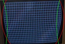
But it's still got an issue. I can't get the geometry into adjustment, specifically the Pin Amp stuff. It's got a fairly complex arrangement for the Pin stuff, so I'm not sure exactly what I should do to fix it. The sides won't go straight. It's got a Pin Low, Pin High, Pin Balance, and Pin Up. I'm not sure exactly what the difference between Low and High is, but it doesn't seem to be able to hit the sweet spot where the sides are straight. It kind of skips over that point and goes wobbly no matter how I set them. I've tried balancing in different ways, but I'm pretty sure at this point that I have an issue. Just not sure what to check.

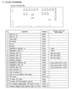
This is the list of the controls I have, and the section of the schematic which shows the Pin Amp stuff. Any ideas on how to check or test this?

Capture.PNGCapturdhe.PNG
 
Basically, the best I can get with the geometry controls at their optimum settings is slightly bowed in on the sides, towards the bottom, or bowed in at the top on the sides.

If I spray some cold spray on the Pin Phase IC303, the screen does jump around a bit and do a dance, so it's possibly getting weird, although I don't know what kind of effect cold spray would have on a healthy IC. Also, it could be cooling down one of the nearby transistors too, it's impossible to only spray one or the other really.

If I had to guess, the issue is the Pin Sides High and Low, which is RV307/310. They do something, but not enough. The other controls seems to do more of what they say they do, if that makes any sense.

This is the best I can get things.

path833.png

OR like this:
path835.png
 
I was able to isolate the TEA2031A Pin Amp IC from the components around it, and it certainly seems like it's the only thing that changes the picture when I spray it with cold. I ordered one because they're cheap, so I will have it to replace if that's the issue.

I removed the two through hole ICs from the board to check underneath and I did not find any signs of pooled up electrolyte or corrosion under them. I think I got lucky with the leaky caps.

My plan is to put a socket in there and test the old IC in circuit to look for waveforms. Not sure what else to try.
 

Attachments

  • stmicroelectronics_cd00019027-1205542.pdf
    105.5 KB · Views: 1
The pincushion correction voltage is supposed to be a parabola shape where the phase of it is such it peaks in amplitude on about the middle of the vertical scan time. So when it is introduced, to modulate the H scan amplitude it can correct the distortion and give a straight side. The pin phase pot will determine the timing of the peak. That looks off because in the image the peak of the curvature is near the bottom of the screen and it should be in the middle of the side of the raster.

The side pin and pin up pots will control the overall amplitude of the correction where they are mixed into the differential amplifier.

If you are getting a sudden jump effect, when you turn the pots rather than a smooth effect it could be poor contact on the wiper of one of the pots is bad.

Ok, thanks Hugo. I'll remove the geometry pots and see how they fair today, although I suspect they are okay.

Another symptom I noticed is that when either of the Pin Side pots is turned all the way down, it stops the Pin Amp controls from responding. It's like turning one of them off is turning them all off.

But I guess if there is a break in one of the pots, then the circuit might behave that way. I just don't think it's the pots though because they are fairly robust cermet types and not the fragile carbon trace ones I often see fail.

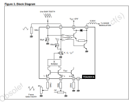
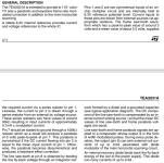
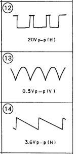
Also, the Pin Amp IC is on the same 24VDC line that blew out before I got to it, so I can't help if it got taken out along the way; the short could have started on the DA board with the bad caps causing a voltage regulation issue and burning out the Pin Amp IC. I want to test it, but not sure what the smoking gun would be. The Pin Amp section of the schematic is two posts back, and here's the excerpt from the datasheet, if you can think of a good test. I have it socketed and can scope the pins once I finish testing the pots. I included the waveforms from around Pin Amp chip on pins 5,7,8 (waves 12,13,14)


block.PNGdescription.PNGwaves.PNG
 
Last edited:
I verified that all the Pin Amp potentiometers are the correct resistance and operate smoothly along their travel.
 
I tested the Pin Amp IC.

Pin 5) correct. 20 Vpkpk square wave @ 31.15kHz

Pin 6) correct 20VDC on it

Pin 7)14VDC offset from schematic is present, but the 0.5Vp-p waveform is screwy and wrong. It looks more like a sawtooth than what the schematic shows, and it's only about 250mV, not 500

Pin 8) 3.4 V pkpk sawtooth. Very close to the 3.6V pkpk shown in the service manual.

So from this I can conclude that something is fishy around the chip or inside the chip. Pin 7 is connected to ground through a 150k resistor, but in this set, it's also connected to the rest of the circuit through a 470k resistor with a cap to ground between them. I have no idea why it's done, but I can guess that maybe it's some kind of DC restoration to bring the level of the chip up to the rest of the circuit on pin 7 or possibly to enable some of the other geometry controls in some way.

Pin 7 is connected to Pin 5 through the one resistor, and the waveform on Pin 5 looks correct, so therefore, I'd basically assume that there's either something wrong with the chip, or with one of the components going to ground between the Pins.

R376- 150k - to GND from Pin 7

C340- 0.0015 - to GND from Pin 7

R375- 470k - between Pin 7 and Pin 5

I have a new Pin Amp IC in the mail, but I'm game to try something else in the meantime. I have the IC socketed, so I can potentially pull Pin 7 and try to create a little circuit with new components that I can put to GND and Pin 5 or something like that.

Does this result say anything to you about the circuit or the failure I'm seeing; it's like something in the circuit is bring down the 500mVpkpk parabola I'm supposed to see to ~280mV and squishing the top down into noise.

Thanks
 
Last edited:
I did a little bit more investigation and I have a little more to add.

I scoped Pins 1 and 2 on IC303 (the Pin Amp IC). I see what appears to be a symmetrical 6.5VDC signal on both Pins, with a small AC component at the refresh frequency.

I also scoped Pin 8 of IC301 (the Horizontal Oscillator), and I see the correct sawtooth waveform there. This is the Pin that supplies the current for Pin 1 of IC303.

My assumption is that components in the circuit between Pin 8 IC301 and Pin 1 IC303 take the sawtooth use it to derive the parabola at Pin 7 with a variable current that is somehow then balanced out on Pin 2 in the circuit. The small AC component I see directly at Pins 1 and 2 is then a reflection of the fluctuating current that is altered by the Pin Amp controls and then derives the final "shape" of the screen, output via Pin 5 of IC303.

When I tweak the Pin Amp pots, I see the small AC component try to wiggle a little bit, but it doesn't change, it just kind of "bounces" back to it's starting state. I am assuming that this isn't correct (the Pin Amp controls should appreciably change the small AC component I see on Pins 1 and 2) and that is a reflection of the issue I'm having.

What I see on the raster is different though; I can see visual feedback when I tweak the Pin Amp pots, although none of them make as pronounced a difference as I would expect them to, and the Side Pins only fix the top of the raster, they don't appear to effect the bottom. The Pin Up control does kind of tweak the top, but only at the very end of it's travel, and it only can make the raster worse.
 
I tried replacing IC303, but I see no change at all. I'm still working on the assumption that there's something wrong with the parabola on the output of Pin 7, but it's worth noting that Pin looks basically okay. If someone could help me understand how the circuit works better, I think I might be able to track it down, but I'm kind of lost right now.

Basically, I need to know what waveforms on the board would be directly effected by the Side Pin controls. If I can scope the spot which reflects that, maybe I can see where things are breaking down. I have been confirming values around IC303 and so far everything looks fine, so I'm thinking that maybe I'm barking up the wrong tree.
 
It would be helpful if you'd post some actual screen shots (ideally showing a grid pattern). There might be something subtle in the image that would give one of us an idea.
 
Sure, if it's helpful I will gladly post it up:

Kw8KxV2.jpg


So this is the output of Pin 5 on IC303. I realize now that the top of it is the key to understanding the pincushion adjustment output. If you look at the top of the waveform, it's supposed to have a flat top that extends past the edges of the square wave evenly on both sides.

This waveform is incorrect as it has the top portion skewed all the way to the left. The waveform wiggles around in a manner that perfectly reflects when I tweak the Pincushion pots, and it snaps back to the left as the sides of the raster similarly refuse to be corrected.

cGyMb8O.jpg


Now I can see why it's displaying incorrectly, but I don't know why or where the problem lies. I've already spent a long time checking voltages, and nothing really seems wrong so far. I've more or less confirmed the values of all resistors, and I checked the ICs that control the mode selection.

Where should I focus my attention?
 
I realize now that the top of it is the key to understanding the pincushion adjustment output.

Not sure how you got that idea. This is not the point of east-west modulation and pin cushion correction.

The point is that the correction waveform, typically a parabolic wave (that is derived from the integration of a vertical rate sawtooth wave) peaks very close to half way down the vertical scan. Your screen image shows that the peak is too close to the raster top, above the center, so correction is impossible. Post #10 was similar in that it showed the peak of the parabola close to the bottom of the scan, albeit with the magnitude of the correction inverted.

It is all about symmetry, not about manipulating the top or bottom of the raster scan.

The point of the phase adjustment is to get the parabolic wave centered about half way down the raster. Then the magnitude of it, is supposed to get the sides of the raster straight. If the magnitude is too low, the pincushion distortion is under corrected, if too high it gets over-corrected and the result is barrel distortion.

So the first move is to get the effect symmetrical with respect to the curve on the side of the raster, and then get the amplitude correct so as to get the sides of the raster straight.
 

Attachments

  • Ew.jpg
    Ew.jpg
    130.1 KB · Views: 4
Last edited:
Back
Top