• Please review our updated Terms and Rules here

CPD1604S Vertical Collapse

Whenever leaking capacitors and corrosion are found, any other problems are almost always directly related. I would go over the board again, looking for open traces, or damaged components. Sometimes it even gets inside ICs and causes them to fail. Also, make sure nothing dripped down onto the main board. Some clear pictures of the board where the leakage was might reveal something.
 
Just because there is no visible corrosion under a part doesn't mean there was no leakage. In the case of the transistor though there will be both leakage between the C,B,E terminals and the tracks under it, the traces running under it are significantly corroded and have lost their coating. There is no escaping the fact that the parts have to be removed for proper surface cleaning, or it will never be reliable.

Also I had been wondering about the magnitude of the H rate serrations seen on the scope recordings of the vertical signals. Some of those can relate to scope probe earthing and some are intrinsic to the design. In this case though leakage currents are almost certainly responsible for a good proportion of it.

Q315 has no damage underneath of it. The solder mask is intact.

FELQ7Rq.png


I removed the surface mount components from the area below the caps in all areas where the solder mask is damaged and ran warm water over it for a couple hours. There wasn't any sign of liquid or film or dirt or anything under any of the parts and there was no damaged solder mask under any of the parts. The only exception being IC304, which is a shunt regulator on the Horizontal Size voltage potentiometer; there was a bit of yellow crud underneath of it.

I did end up with one diode that has a damaged leg now, but it's one of the kind that I ordered so I can replace it.

I also found that two ceramic capacitors have drifted somewhat in value. C327 is supposed to be 220nf and it tests at 300nf, and C329 was supposed to be 0.1uf and it's 0.14uf. Both about 30% off and I guess out of spec. I hardly would think that would crap out the circuit, but I'm willing to consider anything.

Other than that, all transistors seem to test normally on diode test and all resistors appear to be the exact values stated.

I can't do anymore right now because I need at least one of those transistors to replace the one I broke removing everything.
 
Last edited:
Its generally not possible to visually see the electrolyte that causes the leakage trapped under the part, when the part is removed, it is largely transparent . With the board washed under the parts now, most of it should be gone. Hopefully things will come right when you re-fit good parts.

If the transistor & resistors you removed were actually ok initially, then leakage is the only explanation why the emitter follower was not working properly.

It's definitely good to have done it for peace of mind, and I'm happy that the solder mask looks so good underneath everywhere; it's reassuring that it's not a lost cause.

However, I'm also not sure about the health of the transistors in that area. I've definitely run into situations where transistors test fine, but they turn out to be noisy in some way and generally messing something up or causing music to sound wrong in some way. I will replace the old 2SC1623 transistors with the new ones I've got coming while I have the old ones out. I wish I could do it for all of them, but the 2SC / 2SA812 units were not immediately available from Digikey and I wasn't sure enough to order a swap-in.

I've had a transistor go flakey on me that got electrolyte damage on the leg and it crept inside the package and caused just enough havoc to ruin my day.

I know some of these analog circuits really rely on strict values to make things hum. Do you think that the ceramic capacitors are okay that I found to be 30% off of value?
 
I'm not 100% sure how ceramic capacitors are affected by electrolyte. In the case of surface mount resistors the edge of the film can be exposed. With fully encapsulated parts they will be more resistant. But the trouble is, that electrolyte is highly corrosive, attacks most metals, Lead, Tin, Copper, the film in metal film resistors, though it leaves Aluminium alone.

As far as epoxy packages go, the package is supposed to be hermetically sealed, and pin corrosion not enter the part, but, we all know in some cases it does. It has been a reported failure mechanism of IC's. There is a brand of transistor in an epoxy package where they silver plated the wires. The oxidation of the silver coat migrates up into the package and destroys the transistor junction. Presumably, if there is enough electrolyte, the same thing happens with IC's and transistors on surface mount boards affected by leakage, if you wait long enough.
 
Last edited:
I'm not 100% sure how ceramic capacitors are affected by electrolyte.

Regardless of the electrolyte's effects, do you think 30% lower than spec is acceptable in this application?

I know that sometimes caps drift and it has little consequence, but also that there are circuits in which the value is critical and serves a timing purpose or other more exact frequency related roles.
 
30% would be a little on the high range, but monolithic ceramic caps have a fairly wide tolerance in some cases. If they were supply bypass caps I wouldn't think its a problem, but probably any signal coupling caps would be better closer to 10%. Still likely the circuit would still work with them 30% out of range of the specified value, but -30% likely worse than +30%
 
30% would be a little on the high range, but monolithic ceramic caps have a fairly wide tolerance in some cases. If they were supply bypass caps I wouldn't think its a problem, but probably any signal coupling caps would be better closer to 10%. Still likely the circuit would still work with them 30% out of range of the specified value, but -30% likely worse than +30%

Thanks Hugo. I got my transistors today, but I ran into another snag. I broke the leg off of a 2SC812, and I can't find any replacements out there. It's a little SO-23 package, and I managed to find it on a substitution list, but I honestly don't have much experience trying to sub in transistors.

I don't really know what I should buy? Any ideas?

This is the original transistor:


CMENKLL.png


And I found this sub guide from the 1993 Japanese transistor handbook:

16Rt3hJ.png


But I can't really find these, at least not in SO-23 form.

The Toshiba part has different specs from the 2SC812, so I'm a somewhat hesitant. I can't seem to find something new that's exactly like the original.

This is the Toshiba part:

tarGNe1.png
 
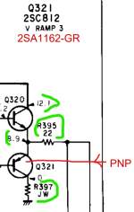
Okay. Scratch that. I realized looking more closely at the schematic that it shows Q321 as a PNP transistor!

If I am remembering correctly, all "2SC" parts are NPN!

So I looked in the parts list at the end, and sure enough it lists a totally different transistor for Q321, a 2SA1162G, which is the Hfe 300 version of that particular part. I am just going to go with that because it looks like this SM has a clear mistake.

Capture.PNG
 
Yes, 2SC, and 2SD are always NPN. 2SA, and 2SB are PNP. In general, for low power circuits like this transistor substitutions are fairly easy. Just get something with equal or greater voltage, and current ratings. Gain shouldn't matter too much as long as it's not wildly different. As you can see from the datasheet, it has a very wide range already. Frequency response isn't a huge concern in this case.
 
Yes, 2SC, and 2SD are always NPN. 2SA, and 2SB are PNP. In general, for low power circuits like this transistor substitutions are fairly easy. Just get something with equal or greater voltage, and current ratings. Gain shouldn't matter too much as long as it's not wildly different. As you can see from the datasheet, it has a very wide range already. Frequency response isn't a huge concern in this case.

Thanks Andy!

Yeah, I just went ahead and got the 2SA1162G parts. Luckily they are still made and still available.

Isn't it just funny how there's still errors in schematics even when it's a reputable company. It's not the only error I've found either; there's a couple of resistors that are the wrong value on the schematic, but correct in the parts list.

Capture.PNG

I got the NPN parts in the mail today, so I already started in on those, and I'll finish up next week when I get the PNPs and an inductor that I broke the leg off of. In fact, I've had a few parts that I broke the legs off of, and they all came from the same area of the board; I'm fairly certain now that the area these transistors came from was more effected by the electrolyte that I thought, and the legs were corroded to the point of the metal weakening. I also got spurious voltage readings in this area. Pretty sure this is where the issue originated.

Hopefully when I get everything back together and turned on, it will fire up and be adjustable. It will have a clean PCB, mostly new transistors and resistors, and a new set of board to board connectors.
 
Errors on schematics are common, so always double check things. I've also seen errors on circuit boards. I make a habit of checking that the board is labeled correctly before I remove a capacitor.
 
On the topic of finding equivalent transistors, it pays to find ones with similar max collector current and voltage ratings and hfe where possible. The problem that crops up in high frequency circuits, including switching circuits is the devices capacitances, storage time and transition frequency are important. So if a part with a larger junction structure and max current and power capability is chosen as a substitute, its capacitances and storage time are often higher.

One major parameter to check is that the transistor's transition frequency is similar to the one being replaced. If the substitute is too low in that parameter it can cause trouble for a particular circuit with switching times as the rise and fall times become delayed, or if too high some circuits become unstable. In a VDU, it is especially important that the HOT has a very low storage time, or the transistor takes too long to cut off for flyback.

Luckily most low power silicon signal transistors have similar enough parameters to be exchanged for near equivalent rated parts, in most of a VDU's signal circuitry. But the ones to watch out for are the HOT and in the video signal circuits, especially the video output transistors driving the CRT, which require more careful substitutes if the originals are hard to get.


Well, I have the transistors I needed, but I just broke the leg off of an 18V zener diode and I don't have any. I could find something the same size, but I do have a bunch of 20V zener diodes. Do you think there's any reason this won't work in this particular circuit?

SJEU1xF.png
 
Last edited:
Okay, scratch all that. I went through my photos and realized that D311 was not populated on my PCB from the factory, so they must have thought it wasn't important. I guess I was correct in thinking that it was just a failsafe and wouldn't really change the circuit.

So I finished putting it all back together and fired it up, but now I have no Horizontal width control, and I've got weird voltages in the area by the Pincushion and the Hor Width voltage.

The 24V supply seems fine as that's there, but there is 24V at the base of Q310 and the Emitter is zero volts. That's giving me no volts on Pin 8 of IC303 and it's not running.

I measured the 15V line back to D304 and it looks like it's 24V there too.

I pulled Q310 and it was blown up inside. Going to replace and see what goes, but I suspect there's something else going on that torched it.

Okay, replacing Q310 got me back to where I was in the beginning in terms of functionality. I now have Horizontal Width control, but the Pincushion is exactly the same as it was before. The Side Pin controls don't have correct effect, and the Pin Up control seems to have a tiny bit, but it's not right. The other Pin related controls have some effect, but none have as much as I would expect them to.

I was able to source the exact replacement transistors for all the 2SC1623 and 2SA1162 and I replaced almost all of them with new ones, so hopefully that took a bit of guesswork out of things. Also, I put in new resistors for everything I took out; I have a kit of Susumi Ultra Precision resistors, so I just figured that would be a good idea. I found a couple of cracked ones, so I thought the electrolyte might have effected things.

This might be a bit of a stretch, but my 12V source line from the D board is down at 11.7V. I wouldn't normally think that's an issue, but maybe it's enough to disturb things?

Trouble is I don't see anything to adjust the 12V source. It's something on the D board L901 DGC, which looks like it takes off of the mains or something. Maybe it's the source diodes going bad?

0VvPS9q.png
 
Last edited:
I replaced the IC303 with another part, and the other transistors in the 300 range, which are largely related to the Pincushion circuit. After getting it back together, I found that I have lost width control, and there is some kind of short or something going on that I have not been able to track down the cause of at all.

The Pincushion IC is connected to the Vert position circuit through Q255, the collector of which is connected to Pin 2 on IC303. It is supposed to be 2.2V at the Collector of Q255, and then end up at 6.5V at Pin 2 of IC303.

Basically what's happening now is that the voltage at Pin 2 of IC303 changes with the Vertical Position pot, which is obviously wrong. I've checked all the transistors and diodes in the area and can't find an issue. I also checked IC205 for shorts between pins and found nothing.

There is 22V at the Emitter of Q254, which will change the voltage present at the bottom of D257, and then raise the voltage at the base of Q255, which finally raises the voltage at the collector of Q255 and that voltage shows up on Pin 2 of IC303.

Any ideas?
YOEec95.png
 
Thing have gone from bad to worse. Now I'm barely getting any image on the raster at all, and there is an area that's got the wrong voltages going on. I've been doing the best I can, but I could really use a hand.

There are two main areas that seem to an obvious problem, and they are connected to each other.

-IC604 has a single bad voltage on the input side; Pin 1 is supposed to be 6.5V, but it is zero volts.

Pin 1 appears to be fed by the 12V rail, through a network of resistors and diodes, and something is obviously bringing it down, but I can't figure out what. IC250 and IC302 are fed by the logic of the network coming from IC604, and I can see there is some obvious issues with them that seem consistent to both ICs. Pin 10 on both ICs appears to be very close to the voltage level of Pin 9, which is connected internally to the collector of their diode networks.

I removed IC205 and IC302 from the board and tested them, and they test identically to a new part on diode test setting of a multimeter.

This is my first time looking at diode networks, so I'm not really sure what should or shouldn't be happening with all of these voltages. It's getting overwhelming.

I have replacement ICs for the diode networks that I can try if it looks like a good idea.

-The other area with an obvious problem is Q317, which is getting fed the erroneous 16.5V on it's collector and emitter, which should be 0.6V each. The base is supposed to be 1.2V and it's closer to 20V. The base is connected to emitter through a diode, so I guess it makes sense that it would be a higher voltage since the C and E are also higher. I don't really understand how this diode is suppose to be employed here though.

I checked the voltages on the other ICs and they basically all look right other than the Pin Amp IC (IC303) which still has bad voltage on Pin2, and Pin 7. It seems pretty likely that the issue is just the bad voltage on Pin 2. Pin 2 is fed by the area of the circuit I'm seeing the bad voltages on. Specifically by Q255, which connects to the Vertical controls stuff. If I mess with the Vert Position, it varies the voltage on Pin2 of IC303


I am struggling with where to focus on here. A point in the right direction would be most appreciative.

This is my erroneous voltages:

KxBVEH0.jpg

This is D609 that feeds Q615 and goes to the base of Q613:
DQFelQo.png


This is logic table for IC604, showing that the bad voltage on Pin 1 makes sense with it's output logic.

pxbhIdS.png


This is what IC250 and IC302 look inside:

N5uVcGq.png


Thanks in advance for any help.
 
Last edited:
I was able to get things back to a place where I have the raster again, but there is still no Pincushion control and there is now almost no Vertical Position adjustment.

The weird voltages might be explainable by the area on the D board that produces the Vertical Position signal which goes to the base of Q255 and the anode of D257. It's supposed to be 8.3 volts, but it's 1.3V.

Either this is throwing off the whole areas near IC250 and IC302, or it's being throw off by that area, I'm not completely sure.

My assumption is that it's coming from the D board because I think Q255 is supposed to be getting it's voltage from the Base side.

Can anyone weigh in on whether or not this sounds correct re the problem is on the D board side VS on the DA board side?

TIA

This is what I'm seeing there:

4s7KRMN.png

pIyNfiv.png
 
If the V POSI signal really is 1.3V (and not 8.3V), the the emitter voltage of Q203 should be about 2V, if it is 8.8v (where you said "okay) then the base-emitter junction of Q203 must be destroyed as it has 7.5V across it in the fwd direction. Check Q202 as well and the fusible resistors.

With all the voltages on Q254 being 24V, this suggests a defect in the V POSI 2 signal, that is supposed to be 7V and instead its 24V, that cuts off Q254 (if the transistor is working), so investigate that too. In the case that Q254 was cut off though, one would expect the collector voltage of it to be lower than 24V, as something should be sinking current to ground in the collector circuit, unless the cause of that fault is a totally shorted out Q254 could explain the measurements.

Probably Q255 is ok, but is base voltage the V Posi signal is simply too low.

The diodes inside the digital transistor arrays with their cathodes connected to the common rail, normally the power rail, are to prevent the collector voltage of the transistors exceeding the supply voltage. In most cases it wouldn't in a circuit with passive components, but it can if say the transistors are used to drive a small inductive load like a small relay coil it can after the coil is de-energized.

Diodes D608's, D609 are wired as a form of OR logic gate where the diode with the lowest cathode voltage of the three, takes control of the common anode voltage, because by lowering the anode voltage it tends to take the other two diodes out of conduction. So the diode with the lower cathode voltage is the main "controller" of the voltage at the junction of the anodes. For example when D609's cathode gets grounded, it kills the current sourced by the two diodes of D608 and the 10k resistor from the 24V rail to the circuits that D608's cathodes feeds.
 
Last edited:
Back
Top