• Please review our updated Terms and Rules here

Intel 4040 little or big endian?

No idea what definitions [of "byte"] were valid when the 4004 came to market...
Varying, I would say. I am just reading A new architecture for minicomputers—The DEC PDP-11 by Gordon Bell et al., presented at AFIPS Spring Joint Computer Conference in May 1970; this was the year before the release of the 4004. On the second page the authors describe the computer as "addressing up to 2¹⁶ eight bit bytes of primary memory." That in 1970 they felt the need to specify that these were eight bit bytes indicates to me that it wasn't until the mid-1970s, at the earliest, that bytes were almost invariably assumed to be eight bits.
 
Any cites for six-bit bytes? My point is that after S/360, the common definition of byte was pretty much established.
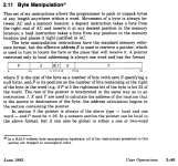
Well, for a start the PDP-10 architecture, introduced in 1968 and with new models throughout the 1970s, had byte addressing instructions such as LDB (load byte), DPB (deposit byte) and IBP (increment byte pointer) which used arbitrary size bytes as specified by the programmer. For more information, see "2.11 Byte Manipulation" in the 1982 DECsystem-10/DECSYSTEM-20 Processor Reference Manual, PDF page 143.

Use of 7-bit bytes on this machine was apparently common as it was a standard size for the OS:

It was common to use 7-bit byte sequences for ASCII text, which gave 5 characters per [36-bit] word and one (usually) unused bit.

There were monitor calls (system calls) that accepted strings of 7-bit characters packed in this way.

So: at the hardware level, bytes were variable-sized. At the software convention level, a byte was frequently 7 bits.


1707111339691.png
 
I remember working with PDP-10 tapes, but I wonder if this use of "byte" to mean 7 bits was an aberration.

Consider the range of mainframes still using 6 bit codes (Univac, CDC for example). Univac 1100 (36 bit) series refers to the 6, 9, 12 or 18 bit word segments as "fields" and the term "byte" never comes up. CDC 6000 (60 bit) never refers to "byte" at all, aside from 8-bit treatment on peripheral devices. Does the literature for the PDP-8 refer to "byte" as anything other than 8 bits?

What I'm getting at, is the PDP-10 use of "byte" something that everyone at the time did? Or was the prevailing idea that "byte" was an 8 bit field? CDC STAR (1969, 64 bit words) refers to "byte" only as 8 bit.
 
Does the literature for the PDP-8 refer to "byte" as anything other than 8 bits?
Sure. The PDP-8/E BSW byte swap instruction swaps two 6-bit bytes between the top and bottom halves of the accumulator.
1707160602284.png
Or was the prevailing idea that "byte" was an 8 bit field?
It seems clear it was not, given that people felt it necessary even in the very early '70s to specify when they meant an 8-bit byte when discussing a new architecture, and that existing architectures had 6-bit and variable-length sub-word fields that they referred to explicitly as "bytes."
 
Addresses are fetched with the lsb nibble first and the high nibble second. This is for the jump instruction of the 4004/4040.
Hope that helps.
Dwight
 
FIM / SRC / FIN, but they all treat registers as register pairs. Pair 0 would be R0 R1 and would be R0=bits 4-7, R1=bits 0-3.
 
I need to clarify what I said, it looks to be confusing.
The ROM is just byte wide memory.
The 4004 fetches a byte at a time, as two cycles on the bus. The high nibble of the byte from ROM is the high part of the instruction. The lower half nibble of the same byte address is the low nibble part.
In the case of a JUN, the lower half, of the high nibble, would be ANDed with $0F and then multiplied by $100 ( a left shift ). This becomes the high part of the destination address.
The next byte is read in and simple ORed with the high part of the address. There is no concept of endedness, as the instruction is in the first byte and any modifier is in the next sequential byte. It follow from high nibble to low nibble as it is in the ROM.
Above, the JUN destination address's highest nibble is the lowest part of the instruction.
I hope that is clearer.
In my simulator, the JUN instruction looks like:

: JUN
CurInstr ( just fetched ) $0F and $100 *
(PC) ( pre-incremented by CrInstr fetch ) $0FF and or
IncPc PC! ;

Looking at my code I don't think the $0FF and is needed as (PC) is a byte fetch not a 16 bit fetch and would be and ended fetch.
If you don't know Forth, you can ignore the above.

Where things become difficult is when a byte is fetched into a register pair. Which nibble gets which part of the byte. I'll describe that next.
Lets look at the FIN instruction.
The byte is fetched. Lets say the register pair was RP1. That will load register R2 and R3.
The High nibble will go into R2 and the low nibble will go into R3.
It seems a little backwards but that is what is does.
My Forth code looks like:

: RegPr! ( n rp - ) \ rp from instruction without right shifting
$0E and Registers + >r \ save destination
dup $F0 and $10 / r@ c! \ '$10 /' is a shift to get high nibble
$0F and r> 1+ c! ;


So, as you said, address areas expected but register pairs are not as expected.

Now that you have a simulator, you can simulate some real world code. Doing this,you will learn what I call instrumenting your simulator with a real world application and not just some trivial "add two numbers together".
get the code at: bitsavers.org/components/Intel/MCS4/Pittmam_MCS4_Assembler.zip
It is a two pass assembler as describe in the user manual in the same directory. For external hardware, it expects there to be an ASR33 teletype with a paper tape punch for output and a paper tape reader for the source data, the intermediate first pass output and the final data in BPN ( or BNP ) format as used for the Intel ROM creation.
It would run on a SIM4-01 as described in the manual. I suggest that you code the paper tape reader and punchers to be files on the machine you are on. Also, in your simulator you find the serial IN/OUT code in the assembler and attach it to your file system rather that taking the bit stream and matching the machine loop timing of the original code but that is up to you as to how realistic you want your simulation to be.
On my simulation I take the bit streams for the second pass and convert the data in bytes to put into a Intel Hex file but that is just cream on the top.
Like I say, this is what I call instrumenting the simulation. It is actually using the simulator for a real world application, otherwise your simulator is just a toy,like any of the other simulators I see on the web for the 4004.
When you get done, note how you connect real world simulations to your simulator and write up how you connect to your simulator. You might think how to script such instrumenting for someone else to use for their project.
Dwight
By the way: I've run this code on my simulator but I don't expect anyone else to use it so I don't have an instruction manual on how to connect to it. I've used my simulator for two real world application so far. This code and the recreation of my Maneuver Board code, that I had to hand patch from a poorly printed listing in a non-intel assembler. The original Maneuver Board would have been in 13 ea 1702 EPROMs when originally written by a student of Gary Kildall. It is interesting code as it uses the CORDIC algorithm to solve the trig problems of Tangent, Sine and Cosine. I've made and actual Electronic Maneuver board but use a 2732 instead of 13 ea 1702s!
For the assembler code, I was able to locate the 4 1702 EPROMs with the original code that Intel used. I wanted to make sure there was no bit rot. Some of the data didn't look right but it worked as expected in the simulation! The EPROMs were likely made in the 1970's and I got them about 3 or 4 years ago from a friend in Europe.
Dwight
 
Thanks Dwight; that gives me a lot to work through. I did run the test chip 4001-0009 after correcting it (the image at http://e4004.szyc.org/emu/ had errors and bit rot along with an error in the Intel manual. A guy received an actual IC of it and dumped it and pointed out the errors. My emulator ran through this and after adding some test code to it, output the same waveform as seen in the Intel document. I'm going to try to implement intel hex loading tonight.
 
>So, as you said, address areas expected but register pairs are not as expected.

I somewhat see the JUN a little differently. It is two bytes, but if you think of it as sequential nibbles, we have high middle low. Yes the highest 4 bit nibble is the low part of the first byte contain the instruction opcode, but bits in opcodes just get put where they get put. I was thinking more about the address nibbles in relation to each other which is where it does high middle low which I tend to think of as big-endian even though these are nibbles and not bytes. This is then consistent with the "big-endian" nibble handing done with the other instructions like FIM/FIN/SRC in regards to the registers.

I've pretty much resolved myself into thinking that endianness doesn't really apply to the 4004, at least not the byte endianness we are used to talking about.
 
I've pretty much resolved myself into thinking that endianness doesn't really apply to the 4004, at least not the byte endianness we are used to talking about.
Exactly my point!

Really, if data were truly little endian, the lowest order bit would be at the lowest address+offset.
 
Is there any more documentation for bitsavers.org/components/Intel/MCS4/Pittmam_MCS4_Assembler.zip?
 
Is there any more documentation for bitsavers.org/components/Intel/MCS4/Pittmam_MCS4_Assembler.zip?
It 's usage is described in the Users Manual. in Appendix F.
The SIM4-01 schematic is on the manual pages 66 and 67.
The ASR33 serial to the printer is on the upper right of 67 and uses a real 4002 output as shown in the schematic.
The serial in comes in on the lower left of the schematic on page 66.
This emulates a ROM output with a dual 4 bit mux, A34. In software you can assume it is a 4001 at the first ROM address.
The assembler assumes you have 2 to 4 4002 RAMs. In order of 4002-1, 4002-2, 4002-1 and 4002-2. I don't recall if it wanted them is a different order but if you have to add them to your simulation you might as well use all 4 as that gives you the most names for address location. As I recall it expects a minimum of 3 RAMs.
The assembler has a more complete description in the Assembler Manual, in the same directory.
Dwight
I have a listing file but it is not in a typical assembler format. It does include labels ( meaning less ones, like L045, for the 45th label I assigned in my disassembler )
It also does code in RPN Forth format like " 0B LDM " which in the normal assembler would be like " LDM, 11 ".
My listings are always in hex.
A typical lines might look like:

0212 52 L046 ZERO INV JCN \ 0252
0213 Label L047 \ 0001
0213 A9 R9 LD

The number at the end of the end of the JCN line is the address of the label L046.
ZERO INV JCN would be jump on the condition of not zero.
The number at the end of the label line, after the slash, is how many time that label is referenced in the program.
I don't recall if the ROM assembler used decimal or hex but it seems I recall it used decimal. I'm sure the manual tells you which.
The listing is too big to put here but if you really want it in the form it is in, I can send it in email. You can put your address in a PM to me.
Dwight
 
After looking at the documentation for the assembler, I am pretty impressed with how fully functional it is!

Dwight, did your simulation convert the bit banged signals on the output 0 pin and test pin back into serial?
 
After looking at the documentation for the assembler, I am pretty impressed with how fully functional it is!

Dwight, did your simulation convert the bit banged signals on the output 0 pin and test pin back into serial?
I don't recall but I think I did it both ways by trapping the call to the serial In/out and also trapping the serial bit changes and looking at the cycle count. Or, once the start bit, I'd set a trigger at a particular cycle count then send or receive each bit.
I did the bit timing first but I did it, later, by trapping at breakpoints at the serial In/out calls of the code.
Both are valid ways of doing it but sometimes it can catch you if you don't do the full bit banging.
It wasn't on this code that I learned no to shortcut when first working with new code. On my Maneuver Board project I trapped all the I/O routines but for the display, it used a number of 7 segmented LEDs for the calculation outputs and entry. For the outputs, I took the data straight from the RAM array and printed it out on the screen. When I got around to making the actual hardware, I assumed, for some reason, I can justify that the display was scanned left to right. Well after building the actual calculator in hardware, I found the code scanned the display right to left. Since the display was layed out as 3 rows of different lengths, it made it not work too well.
I had a choice. I could do some more cuts and jumpers or modify the software to scan the other way. I'd already did enough cuts because of some package layout errors I wasn't to happy to add more so I modified the software.
Anyway, doing to much short cutting in the simulation can sometimes catch you in the lie of thinking you are truly doing the full simulation.
Anyway, it worked well in the end. I even found a bug in the operation. If the Own Ship was on a course of 0.0 degrees the calculations would be off by a lot. I suspect that any course that was on the 4 compass points would do the same, knowing how the CORDIC method works. It did well enough if one just did +- 0.1 degree from the exact value on the 4 compass points.
It was cleaver software as it could track 10 vessels at a time, all running on a 4004 and doing complicated trig in about 6 seconds.
Dwight
 
Back
Top