nikola-wan
Veteran Member
Tektronix introduced their second generation 4050 microcomputers in 1979 - the 4052 and 4054.
Both of these computers were at least 8x faster running Tektronix 4050 BASIC programs than their first generation 4051 introduced in 1975 which had a Motorola 6800 CPU with a clock speed of 800KHz.
Bob Haas designed the bit-slice CPU for the 4052 and 4054 and described the design goals in his VintageTEK youtube video:
Tektronix 4052 Development and Speed Comparison to 4051
4052/4054 CPU Design goals
Engineering proposed and management supported incorporating the double-precision floating point operations in microcode. This also would require extensive changes in the BASIC ROMs to use the new microcode instructions.
Bob added new opcodes for 4050 BASIC 64-bit floating point in the unused spaces of the 6800 instruction set and the result was over 30x speedup for floating point computations which also resulted in 8x speedup in vector graphics performance due to the multiple floating point operations to draw any vector!
Result
The 4052 and 4054 exceeded the goal of 8x performance improvement for the launch in 1979.
The third generation 4050 computers were named 4052A/4054A and launched in June 1982 with more new opcodes in the bit-slice CPU providing a 20% performance increase for some BASIC commands. These computers also included faster GPIB and serial interfaces, and new 4050 BASIC commands including structured BASIC and several new graphics commands - see this article:
Tekniques Vol6 No3 - BASIC Language Enhancements Highlight New Models
The next Tekniques Vol6 No4 included a tape with a 4052A/4054A Assembler written by two Tektronix programmers using the new structured BASIC commands.
I inventoried a large collection of Tektronix manuals and tapes at the Living Computer Museum in Seattle in 2018 and found that tape in the collection! I filled out a request to try to recover that tape and a couple of other tapes in that collection and recovered the entire tape and got LCM to scan the documentation for that tape and posted the assembler BASIC program and documentation on my github repository in this folder:
4052A-4054A-Assembler
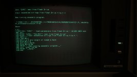
The assembler documentation is 97 pages and includes not only the new opcodes for the 4052/4054 but also the opcodes added for the 4052A/4054A. It includes a couple of short programs to assemble and run - I also got Motorola MIKBUG assembled and running on my 4054A.
Most of the documentation is detailed descriptions for each new opcode and a list of 4052A/4054A BASIC ROM entry points!!
As I have been trying to disassemble the Option 30 Dynamic Graphics Coprocessor firmware - I will also need to understand how the 4054A sends commands to the Option 30, so I am examining the 4052 Assembler documentation again.
I found a nice Motorola 6800 opcode table here:
6800 instruction set
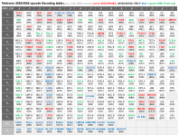
I put the table into a Word document and created a Tektronix 4052/4052A 4054/4054A opcode table from the BASIC assembler program and the assembler document:

As you can see - Bob Haas added the opcodes in RED in the 6800 opcode gaps which have a GREY background color in addition to all the 6800 opcodes in BLACK to the original 4052/4054. Bob told me he did not work on the 4052A/4054A ALU, but the opcodes in BLUE and GREEN were added in addition to keeping all the opcodes in BLACK and RED.
The GREEN opcodes are 6800 backwards compatible 16-bit extensions to operations on the A and B accumulator registers.
The engineers ran out of gaps for all the BLUE opcodes added for the 4052A/4054A and added C7 and FC as escape prefix codes to support the two extra lines in the opcode table for a total number of opcodes of 275 !!!
Here is my list of register extensions for the original 4052/4054 and 4052A/4054A with the same color codes as the opcode table:

Since they doubled the RAM and ROM sizes to 64KB - they were still limited to the 16-bit address lines so they added opcodes to change the address to/from the new Data Space A and Fetch Space B - and added condition code bits to detect which space is currently selected.
The assembler document indicates that this is the reason the assembly programs need to use SWI before accessing the ROMs - and the microcode will switch the space from RAM to ROM. The RET instruction will return from ROM space back to RAM space for the assembly program.
Both of these computers were at least 8x faster running Tektronix 4050 BASIC programs than their first generation 4051 introduced in 1975 which had a Motorola 6800 CPU with a clock speed of 800KHz.
Bob Haas designed the bit-slice CPU for the 4052 and 4054 and described the design goals in his VintageTEK youtube video:
Tektronix 4052 Development and Speed Comparison to 4051
4052/4054 CPU Design goals
- 6800 compatibility
- Must be able to leverage the 4051 32KB BASIC ROM firmware development
- 8 times faster than the 4051
- 3 Factors of Two
- Double CPU clock speed (2MHz vs 800KHz)
- Double memory bandwidth with 16-bit memory width
- This also doubled the address space which doubled the RAM to 64KB and doubled the ROM space to 64KB!
- Harvard Architecture - overlap instruction and data fetch
- 3 Factors of Two
- 6800 8-bit instructions and data could not take advantage of 16-bit memory bandwidth speedup
- Harvard architecture was challenging and not delivered at launch in 1979
Engineering proposed and management supported incorporating the double-precision floating point operations in microcode. This also would require extensive changes in the BASIC ROMs to use the new microcode instructions.
Bob added new opcodes for 4050 BASIC 64-bit floating point in the unused spaces of the 6800 instruction set and the result was over 30x speedup for floating point computations which also resulted in 8x speedup in vector graphics performance due to the multiple floating point operations to draw any vector!
Result
The 4052 and 4054 exceeded the goal of 8x performance improvement for the launch in 1979.
The third generation 4050 computers were named 4052A/4054A and launched in June 1982 with more new opcodes in the bit-slice CPU providing a 20% performance increase for some BASIC commands. These computers also included faster GPIB and serial interfaces, and new 4050 BASIC commands including structured BASIC and several new graphics commands - see this article:
Tekniques Vol6 No3 - BASIC Language Enhancements Highlight New Models
The next Tekniques Vol6 No4 included a tape with a 4052A/4054A Assembler written by two Tektronix programmers using the new structured BASIC commands.
I inventoried a large collection of Tektronix manuals and tapes at the Living Computer Museum in Seattle in 2018 and found that tape in the collection! I filled out a request to try to recover that tape and a couple of other tapes in that collection and recovered the entire tape and got LCM to scan the documentation for that tape and posted the assembler BASIC program and documentation on my github repository in this folder:
4052A-4054A-Assembler
The assembler documentation is 97 pages and includes not only the new opcodes for the 4052/4054 but also the opcodes added for the 4052A/4054A. It includes a couple of short programs to assemble and run - I also got Motorola MIKBUG assembled and running on my 4054A.
Most of the documentation is detailed descriptions for each new opcode and a list of 4052A/4054A BASIC ROM entry points!!
As I have been trying to disassemble the Option 30 Dynamic Graphics Coprocessor firmware - I will also need to understand how the 4054A sends commands to the Option 30, so I am examining the 4052 Assembler documentation again.
I found a nice Motorola 6800 opcode table here:
6800 instruction set
I put the table into a Word document and created a Tektronix 4052/4052A 4054/4054A opcode table from the BASIC assembler program and the assembler document:

As you can see - Bob Haas added the opcodes in RED in the 6800 opcode gaps which have a GREY background color in addition to all the 6800 opcodes in BLACK to the original 4052/4054. Bob told me he did not work on the 4052A/4054A ALU, but the opcodes in BLUE and GREEN were added in addition to keeping all the opcodes in BLACK and RED.
The GREEN opcodes are 6800 backwards compatible 16-bit extensions to operations on the A and B accumulator registers.
The engineers ran out of gaps for all the BLUE opcodes added for the 4052A/4054A and added C7 and FC as escape prefix codes to support the two extra lines in the opcode table for a total number of opcodes of 275 !!!
Here is my list of register extensions for the original 4052/4054 and 4052A/4054A with the same color codes as the opcode table:

Since they doubled the RAM and ROM sizes to 64KB - they were still limited to the 16-bit address lines so they added opcodes to change the address to/from the new Data Space A and Fetch Space B - and added condition code bits to detect which space is currently selected.
The assembler document indicates that this is the reason the assembly programs need to use SWI before accessing the ROMs - and the microcode will switch the space from RAM to ROM. The RET instruction will return from ROM space back to RAM space for the assembly program.
Last edited:

