• Please review our updated Terms and Rules here

Tektronix 4054A with Option 30 Dynamic Graphics coprocessor - won't boot to BASIC

nikola-wan

Veteran Member
Joined
Mar 7, 2018
Messages
1,410
Location
Texas, USA
VintageTek Museum in Oregon has a Tektronix 4054A computer with Option 30 Dynamic Graphics coprocessor that they have been restoring.

What works:
  • Without the Option 30 board, their 4054A boots BASIC and run programs from a Flash Drive that I donated to the museum along with a Jos Dreesen Multifunction ROM Pack.
  • With the Option 30 board installed and Jos Dressen's 4052/4054 Diagnostic ROM Pack installed and set to run the Option 30 RAM test, the test shows Option 30 RAM is OK

What fails:
  • With the Option 30 board and Diagnostic ROM - after the Option 30 test (or any other Diag test), the 4054A is hung and does not return to BASIC and instead of a rectangular blinking cursor - they just get a dot where the cursor should be
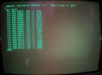
Here is their photo of their 4054A after the Option 30 Memory Test:
VintageTek Option 30 Diag Test.jpeg

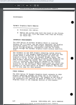
The error message after the Option 30 MEMORY TEST is NOT a problem with the Option 30 MEMORY, it is listed in the 4052 Diagnostic ROM Pack manual page 18 as happening after the test if the 4054A only has 32KB of RAM:
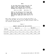
1729947264306.png

What is an error in the Option 30 MEMORY test photo is the GREEN dot above the OPT 30 TESTS - this should be a blinking cursor rectangle.

The fact that the Option 30 MEMORY test ran with no errors indicated the Diagnostic ROM was able to communicate with the Option 30 8x300 coprocessor and successfully read/modify/write the Option 30 32KB of RAM.

This communication uses the PIAs on the I/O board to generate commands to the Option 30 and read the results from Option 30.
These same PIAs are used to control the Display and Vector boards to move and draw vectors including the vectors in text - so that hardware is also working - even when the Option 30 board is present.

The Option 30 Operators Manual including the Quick Reference Guide and Service Manual is located here:
https://w140.com/tekwiki/images/1/1c/070-2289-02.pdf

The next photo from the VintageTek museum shows using the Diagnostic ROM Pack to perform a ROM CRC test on the 4054A BASIC ROMs - which match my 4054A BASIC ROMs v1.5 (except for my MFM pack in the second slot so UE51A and UE51B show non-zero CRCs).
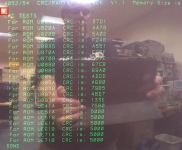
VintageTek 4054A CRC test.png Monty 4054A CRC test.jpg

Note my screenshot on the right shows the blinking orange (Option 31 Color Dynamics CRT - which is installed in both computers), but the left image shows a orange dot - not blinking, and the VintageTek computer BUSY light is on and the computer is hung.

So the VintageTEK Option 30 issue appears to be associated with the blinking cursor.

Without Option 30 installed - the blinking orange cursor is displayed, which is done in BASIC ROM firmware.
With Option 30 installed - the cursor is done by the Option 30 board and the cursor can be changed to any Option 30 object as indicated on this page of the Option 30 manual:
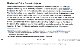
1729948653995.png

This Option 30 manual page indicates there are several different Option 30 object numbers can be used as the cursor, in addition to a user defined object number:
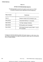
1729948953883.png

My suspicion is something is wrong with their Option 30 ability to blink the cursor.

I have burned a new set of Option 30 PROMs, tested them on my Option 30 and sent them to vintageTEK museum, but replacing the PROMs did NOT fix the cursor problem.

My Option 30 is working so I could capture logic analyzer data if that helps.

They have a logic analyzer and were looking at the PROM signals.

Does anyone have suggestions on our next step to repair their Option 30?
 
Last edited:
I talked to vintageTEK and outlined where I think they can start to debug their OPTION 30 issue that hangs the BASIC ROM after running the Diag ROM Option 30 test - or any other Diag ROM test - and is likely the same issue that hangs the BASIC ROM if OPTION 30 is installed without installing the Diag ROM pack.

My theory is:
  • 4054/4054A BASIC ROM detects presence of OPTION 30 board during power up by reading the Display board status byte
1730041798185.png

  • I believe the status bit in question is bit 2 (third bit) based on this bit set to ground in the Option 30 DSTAT buffer:
1730042511284.png

  • Without the Option 30 board installed, I believe this bit will be logic High returned from the Display board
  • With Option 30 board installed, the BASIC ROM will detect the Option 30 and if the Diag ROM pack is installed - the Diag ROM Pack will perform a test based on the DIP switch setting on that ROM pack
  • After the Diag ROM Pack has finished the test - or if no ROM Pack is installed - the BASIC ROM will then attempt to display the rectangular blinking cursor.
    • If no OPTION 30 board was detected, the BASIC ROM code will draw the blinking cursor in refresh mode
    • If OPTION 30 was detected, the BASIC ROM will program OPTION 30 to draw and blink the cursor
This is the point the vintageTEK 4054A hangs if OPTION 30 installed, so I requested they start their debug at the OPTION 30 DSTAT buffer.

This buffer is likely working as the BASIC ROM only hangs with OPTION 30 installed. But looking at when this buffer is active will be a start on debugging what happens after that.
 
I believe we may need the Option 30 PROM code to be disassembled in case we need to track the code execution to find the problem on the board.

@stepleton found and began using a 8x300 CPU disassembler in this vcfed post:
https://forum.vcfed.org/index.php?threads/tektronix-4050-gpib-flash-drive-now-available.1238891/post-1265525

I used the sequence of PROMs in his post and got this disassembly listing, and began adding my comments on how the Option 30 board uses the third pair of PROMs - based on the great information in the Option 30 service manual Theory of Operation.

Code:
; Tektronix 4054/4054A OPTION 30 PROM code disassembly using github.com/brouhaha/s8x30x - 27OCT2024 MCM
;
; I used ALL-100 Universal Programmer - Utility | 2-way shuffler to create the BYTE shuffled input files as follows:
; OPT30M.bin = U495 for OPT30M.EVN and U375 for OPT30M.ODD
; OPT30L.bin = U385 for OPT30L.EVN and U475 for OPT30L.ODD
;   per Tom Stepleton's table in
;   https://forum.vcfed.org/index.php?threads/tektronix-4050-gpib-flash-drive-now-available.1238891/post-1265525
; OPT30F.bin = U485 for OPT30F.EVN and U395 for OPT30F.ODD
;
; and then used this command to the disassembler in WSL Ubuntu 20.04 Linux (since OPTION 30 uses the 8x300 CPU):
; ./dis8x30x --wd1000 -l OPT30M.bin OPT30L.bin OPT30F.bin >OPT30.dis
;
; The // comments in the listing are the decodes of the third byte OPTION 30 IV bus bits
;
; NOTE in s8x30x disassembler SYNTAX in the README:
;  Bit positions are designated with bit 0 as the least significant bit
;  and bit 7 as the most significant bit, which is the opposite of the notation Signetics uses,
;  but matches almost everything else using microprocessor and peripheral chips,
;  including the I/O on the WD100x disk controllers.
; 
; The Tektronix 070-2289-02 NOV 1982 4054/4054A OPT. 30/31 Operation/QuickRef/ServiceManual
; https://w140.com/tekwiki/images/1/1c/070-2289-02.pdf
;  ServiceManual Theory of Operation pages 4-5, 4-6 and 4-7 describe the OPTION 30
;  Input/Output Destination byte (IOD) which is noted as different than the 8x300 datasheet (page 4-6):
;
;  The IOD byte is the high 8 bits of the 24-bit word from the 8X300 control ROM.
;  The IOD byte allows a different instruction format than those shown in the
;  manufacturer's data sheet. To write data into an IV Bus, or read data from an IV
;  Bus, the Dynamic Graphics board does not require the SC signal or the "Move"
;  instruction for IV Bus selection. Instead, the proper "Move" instruction
;  (write or read format) is located in the lower 16 bits of the 24-bit word
;  from the 8X300 control ROM (Figure 4-3). The IOD byte selects the proper
;  IV Bus byte to be acted upon by the write or read operation determined
;  by the "Move" instruction in the lower 16 bits. In this way the number of
;  instructions needed to move data is cut from two to one. The same operation
;  of the IOD byte is used with all op-code instructions which use data from the IV Bus.
;
; The s8x30x --wd1000 parameter decodes the third byte as Fast IO Select, described in:
; https://bitsavers.computerhistory.org/pdf/westernDigital/WD100x/WD1000_OEM_Manual.pdf
; page 8-1 as decoding to 8-read strobes and 8-write strobes used in the subsequent 8X300
; instruction to read or write 8-bits of data to or from the 8x300 IO bus

; Here is my list of IOD byte values in Tektronix OPTION 30 format:
;
; IOD bit 7 (23) and 6 (22) are OPT30 RAM Memory Control (Table 4-1)
;         0          0      Command/Status/Scratch (does not use RAM)
;         0          1      RAM_READ   
;         1          0      RAM_WRITE   
;         1          1      RAM_REFRESH
;
; IOD bits 6 (21) to 0 (16) are Commands or 16 Scratch Pad Registers using IO byte (Table 4-2)
;        00                 Command   to   Display Controller
;        01                 Status    to   4054 Processor
;        02                 HIGH byte to   Vector Generator
;        03                 LOW  byte to   Vector Generator
;        04                 HIGH byte to   4054 Processor
;        05                 LOW  byte to   4054 Processor
;        06                 HIGH byte to   Memory Address Register
;        07                 LOW  byte to   Memory Address Register
;        08                 Command   from 4054 Processor
;        09                 Status    from Display Controller
;        0A                 HIGH byte from 4054 Processor
;        0B                 LOW  byte from 4054 Processor
;        0C                 HIGH byte from Vector Generator
;        0D                 LOW  byte from Vector Generator
;        0E                 HIGH byte from Memory address
;        0F                 LOW  byte from Memory address
;
;        10                 READ           Scratch Register 0
;        11                 READ           Scratch Register 1
;        12                 READ           Scratch Register 2
;        13                 READ           Scratch Register 3
;        14                 READ           Scratch Register 4
;        15                 READ           Scratch Register 5
;        16                 READ           Scratch Register 6
;        17                 READ           Scratch Register 7
;        18                 READ           Scratch Register 8
;        19                 READ           Scratch Register 9
;        1A                 READ           Scratch Register A
;        1B                 READ           Scratch Register B
;        1C                 READ           Scratch Register C
;        1D                 READ           Scratch Register D
;        1E                 READ           Scratch Register E
;        1F                 READ           Scratch Register F

;        30                 WRITE          Scratch Register 0
;        31                 WRITE          Scratch Register 1
;        32                 WRITE          Scratch Register 2
;        33                 WRITE          Scratch Register 3
;        34                 WRITE          Scratch Register 4
;        35                 WRITE          Scratch Register 5
;        36                 WRITE          Scratch Register 6
;        37                 WRITE          Scratch Register 7
;        38                 WRITE          Scratch Register 8
;        39                 WRITE          Scratch Register 9
;        3A                 WRITE          Scratch Register A
;        3B                 WRITE          Scratch Register B
;        3C                 WRITE          Scratch Register C
;        3D                 WRITE          Scratch Register D
;        3E                 WRITE          Scratch Register E
;        3F                 WRITE          Scratch Register F

0000: d7 10 09 x0000:  xmit    10h,dliv     // rd=1
0001: 57 01 02         and     rd2,r1
0002: d7 00 22         xmit    0h,ram_addr_low     // rd=2
0003: a1 04 02         nzt     r1,x0004     // rd=2
0004: c9 00 22 x0004:  xmit    0h,r11     // rd=2 wr=2
0005: c1 85 e2         xmit    85h,r1     // rd=2 wr=6
0006: c4 01 00         xmit    1h,r4     // rd=0
0007: 01 17 22         move    r1,ram_addr_low     // rd=2
0008: c0 3f 22 x0008:  xmit    3fh,aux     // rd=2 wr=2
0009: c0 01 22         xmit    1h,aux     // rd=2 wr=2
000a: 00 17 22         move    aux,ram_addr_low     // rd=2
000b: c9 01 c6         xmit    1h,r11     // rd=6 wr=4
000c: c0 80 22         xmit    80h,aux     // rd=2 wr=2
000d: e6 67 22         jmp     x0667     // rd=2 wr=2
000e: 00 17 43         move    aux,wr_serdes     // rd=3
000f: 1f 17 07         move    sriv,dliv
0010: c0 01 00         xmit    1h,aux     // rd=0
0011: d7 05 22 x0011:  xmit    5h,ram_addr_low     // rd=2
0012: 29 09 22         add     r11,r11     // rd=2 wr=2
0013: c0 02 22         xmit    2h,aux     // rd=2 wr=2
0014: 09 1f 22         move    r11,driv     // rd=2 wr=2
0015: c9 01 a2         xmit    1h,r11     // rd=2 wr=2
0016: a9 08 22 x0016:  nzt     r11,x0008     // rd=2 wr=2
0017: e6 67 22 x0017:  jmp     x0667     // rd=2 wr=2
0018: c0 7f 22         xmit    7fh,aux     // rd=2 wr=2
0019: c1 88 22         xmit    88h,r1     // rd=2 wr=2
001a: 37 00 22         add     rd2,aux     // wr=2
001b: e4 13 0e x001b:  jmp     x0413     // rd=6
001c: 00 17 22         move    aux,ram_addr_low     // rd=2
001d: c1 89 06         xmit    89h,r1     // rd=6
001e: a8 11 22         nzt     ovf,x0011     // rd=2 wr=2
001f: e4 13 22         jmp     x0413     // rd=2 wr=2
0020: e0 08 22         jmp     x0008     // rd=2 wr=2
...

see the attachment for the complete 2KB disassembly listing

The // comments are from the disassembler using WD1000 hard disk controller usage of the third byte.

I'm not skilled at writing python code, but someone skilled in python could probably replace the code in the wd1000.py file which generated the disassembly comments with my Option 30 comments based on the value of the third byte!

Then we would have an Option 30 disassembler
😀
 

Attachments

  • OPT30_dis.zip
    19 KB · Views: 2
Oops, I didn't include the input bin files.

Here is a zip with both input and dis files:
 

Attachments

  • OPT30_dis_with_bin_files.zip
    23.1 KB · Views: 1
I also neglected to mention a couple of labels you see in the disassembly listing:
  • The 8x300 has eight internal registers R1-R6, R11, and AUX (Table 1 in the 8x300 datasheet in the Opt30 service manual)
  • OVF register (overflow from most recent ADD)
  • IR (holds current 16-bit instruction word being executed)
  • PC program counter
  • AR 13-bit address register
  • S (source field) in the instruction
  • D (destination field) in the instruction
  • R/L rotate/length
  • I immediate
  • A address
  • IV Interface Vector used for instructions reading or writing an I/O data field
    • IVL and IVR are write-only pseudo registers only specified as destination
    • Probably not used in OPTION 30 based on the two instruction 8x300 IV example on page A-6
some of these labels are concatenated in the disassembly:

example: 0000: d7 10 09 x0000: xmit 10h,dliv
dliv = destination IVL

similarly:
sriv = source IVR

and several others are WD1000 hard disk controller port decodes:
  • ram_addr_low
  • wr_serdes
  • wr_host_port
etc
 
Last edited:
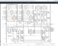
Hmm, I think the OPT30F.bin PROMs are swapped - when I look at the schematic of the Option 30 page A1-2:

1730119074554.png
U495, U385 and U395 have CE2 enabled LOW if 8X300 CPU A2 is LOW, so these PROMs are the OPT30 MSB and therefore the EVEN PROMs.

So I need to reshuffle them and regenerate the "F" file:
OPT30F.bin = U395 for OPT30F.EVN and U485 for OPT30F.ODD

I have attached my 28OCT2024 zip with the reshuffled OPT30F as the third byte.
 

Attachments

  • OPT30-F-reshuffled.zip
    21.2 KB · Views: 1
As I am trying to manually disassemble the Option 30 code - I must first understand how the 8X300 CPU interacts with the Option 30 hardware.

I first thought I needed to reverse the 8-bit bytes in the OPT30F.bin file which byte shuffles U395 and U485 bytes to match the four PROMs containing the 2K words of 16-bit wide code.

However, a closer look at the A1-2 schematic with the 8X300 / PROMS / RAM - I see that all the PROM data bits are swapped in the schematic, so the OPT30-F-reshuffled disassembly previously attached - third byte of each opcode can be directly analyzed on each instruction where bits 7 and 6 are for RAM memory control as described in Table 4-1 and the remaining bits 5-0 are used for decoding I/O ports and the sixteen scratch pad RAM bytes.

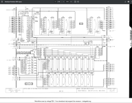
I have been examining the schematic page A1-3 which contains the U530 latch for the I/O register decodes and scratch pad rams and decided to add the I/O register names on that page to my disassembly comments instead of the longer Table 4-1 description for brevity:

Code:
; HEX IOD value of bits 5-0 then First label is schematic signal name.  Second label is from table 4-1
;           x 00     LCDC     Command   to   Display Controller
;           x 01     LSH      Status    to   4054 Processor
;           x 02     LDHVG    HIGH byte to   Vector Generator
;           x 03     LDLVG    LOW  byte to   Vector Generator
;           x 04     LDHH     HIGH byte to   4054 Processor
;           x 05     LDLH     LOW  byte to   4054 Processor
;           x 06     LDHM     HIGH byte to   Memory Address Register
;           x 07     LDLM     LOW  byte to   Memory Address Register
;           x 08     ECH      Command   from 4054 Processor
;           x 09     ESDC     Status    from Display Controller
;           x 0A     EDHH     HIGH byte from 4054 Processor
;           x 0B     EDLH     LOW  byte from 4054 Processor
;           x 0C     EDHVG    HIGH byte from Vector Generator
;           x 0D     EDLVG    LOW  byte from Vector Generator
;           x 0E     EMAH     HIGH byte from Memory address
;           x 0F     EMAL     LOW  byte from Memory address
;           x 10     RSP1     READ  Scratch Pad Register 1
;           x 11     RSP2     READ  Scratch Pad Register 2
;           x 12     RSP3     READ  Scratch Pad Register 3
;           x 13     RSP4     READ  Scratch Pad Register 4
;           x 14     RSP5     READ  Scratch Pad Register 5
;           x 15     RSP6     READ  Scratch Pad Register 6
;           x 16     RSP7     READ  Scratch Pad Register 7
;           x 17     RSP8     READ  Scratch Pad Register 8
;           x 18     RSP9     READ  Scratch Pad Register 9
;           x 19     RSP10    READ  Scratch Pad Register 10
;           x 1A     RSP11    READ  Scratch Pad Register 11
;           x 1B     RSP12    READ  Scratch Pad Register 12
;           x 1C     RSP13    READ  Scratch Pad Register 13
;           x 1D     RSP14    READ  Scratch Pad Register 14
;           x 1E     RSP15    READ  Scratch Pad Register 15
;           x 1F     RSP16    READ  Scratch Pad Register 16

;           x 20-2F are not used

;           x 30     WSP1     WRITE Scratch Pad Register 1
;           x 31     WSP2     WRITE Scratch Pad Register 2
;           x 32     WSP3     WRITE Scratch Pad Register 3
;           x 33     WSP4     WRITE Scratch Pad Register 4
;           x 34     WSP5     WRITE Scratch Pad Register 5
;           x 35     WSP6     WRITE Scratch Pad Register 6
;           x 36     WSP7     WRITE Scratch Pad Register 7
;           x 37     WSP8     WRITE Scratch Pad Register 8
;           x 38     WSP9     WRITE Scratch Pad Register 9
;           x 39     WSP10    WRITE Scratch Pad Register 10
;           x 3A     WSP11    WRITE Scratch Pad Register 11
;           x 3B     WSP12    WRITE Scratch Pad Register 12
;           x 3C     WSP13    WRITE Scratch Pad Register 13
;           x 3D     WSP14    WRITE Scratch Pad Register 14
;           x 3E     WSP15    WRITE Scratch Pad Register 15
;           x 3F     WSP16    WRITE Scratch Pad Register 16

I found 8X300 documents on bitsavers in this directory:
http://www.bitsavers.org/components/signetics/8X3xx/

Including a newer 8x300 datasheet plus Programmer and Applications Guides with lots more description of how to use the 8X300 with examples and a couple of application notes including note AH4 on Fast IV Select to get single CPU cycle instructions that can directly provide the IOD byte as data to a register or RAM - just like the Option 30 manual describes!

Schematic A1-1 generates I/O READENABLE-0 and WRITEENABLE-0 signals from 8X300 LB-0 and WC signals so all I/O registers and Scratch Pad RAM are accessed as Left Bank (LIV).

The Option 30 32KB of DRAM is accessed as Right Bank (RIV).

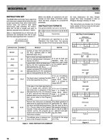
Here is the datasheet page for the 8 opcodes in the 8X300 CPU (really super RISC):
8x300 Instruction Set.jpg

First 3-bits are the opcode followed by 13 bits which provide source, destination, rotate or JMP address based on opcode format.

Here is my first attempt at Option 30 disassembly based on the listings from the s8x30x disassembler without using the -WD1000 parameter:

Code:
0000: d7 10 02 x0000:  xmit    10h,dliv    // Write 10h to LDHVG    HIGH byte to   Vector Generator
0001: 57 01 09         and     sliv,r1     // AND ESDC (Display Ctrl Status) /w AUX & Write to R1
0002: d7 00 02         xmit    0h,dliv     // Write 00h to LDHVG    HIGH byte to   Vector Generator
0003: a1 04 22         nzt     r1,x0004    // IF R1<>0 THEN JMP x0004  (I think IOD=22 is an IOD no-op)
0004: c9 00 e2 x0004:  xmit    0h,r11      // Write 00h to R11 and perform MEMORY Refresh cycle (?)
0005: c1 85 22         xmit    85h,r1      // Write 85h to R1
0006: c4 01 22         xmit    1h,r4       // Write 01h to R4
0007: 01 17 00         move    r1,dliv     // MOVE R1   to  LCDC     Command   to   Display Controller
0008: c0 3f 22 x0008:  xmit    3fh,aux     // Write 3Fh to AUX
0009: c0 01 22         xmit    1h,aux      // Write 01h to AUX
000a: 00 17 c6         move    aux,dliv    // MOVE AUX to MEMORY Refresh address 0006h?
000b: c9 01 22         xmit    1h,r11      // Write 01h to R11
000c: c0 80 22         xmit    80h,aux     // Write 80h to AUX
000d: e6 67 22         jmp     x0667       // JMP to x0667 (memory refresh routine?)

Not sure I got this far correctly - help appreciated :)
 
Last edited:
In my short disassembly in the last post, I take advantage of the s8x30x disassembler decoding of the two-byte opcode bits and showing dliv, sliv, driv and sriv labels where present in the D and S fields:
  • dliv means destination is LEFT BANK (I/O or Scratch RAM in Option 30, and IOD bits 7 and 6 also indicate memory operation)
  • sliv means source is LEFT BANK (I/O or Scratch RAM in Option 30, and IOD bits 7 and 6 also indicate memory operation)
  • driv means destination is RIGHT BANK (DRAM memory where IOD bits 7 and 6 indicate memory operation)
  • sriv means source is RIGHT BANK (DRAM memory where IOD bits 7 and 6 indicate memory operation)
 
Back
Top