• Please review our updated Terms and Rules here

KIM-1 Repairs continue

Hi All
I'm sorry I've not had a chance to reply. Monday night, I went to bed with a fever. I'd caught the latest version of Covid. I've had it once so there is nothing to the statement that once you've had it you are immune. I'd had the full series of 5 shots but didn't go back for the latest variant shot. My mistake.
I'm mostly over it now, some sniffles is all.
Anyway, the code images on the web page are correct. If you build the diagnostic, I should note that if you run the RAM test and it tells you every other RAM is bad, it is more likely that the main selects for the RAM are the problem and not necessarily one of the RAMs. That would need to be fixed, first.
I use a pattern of 10101010 and 01010101 for the RAM test so if the buss stays at 1 or 0 it will indicate alternate RAMs as failing. I didn't think about this when I wrote the instructions, please forgive me. As you may have guessed, the RAM test is like a chicken and egg problem.You can't use the RAM until you've tested it and the 6502 loves to use the RAM as pointers. This meant that the entire RAM test needed to run in the processors registers. It needed to read/write and report failures using only those registers.

If you look at the sections of the EPROM data, there are two that are mostly the code that goes into the 6530 ROMs on the KIM. It is a problem that I can only address 1K of code at a time, when the debug board is used. I still need to boot to a valid code address and have the code for the EEPROM used on my replacement modules.
This means the reset address at the end of the EPROM 1K block needs to boot to a valid debug code address. So, the 1K block that is the ROM image is complete except the boot address, that is in RAM instead. This was loaded by the previous EPROM 1K block into RAM. When I write to the EEPROM, I patch the correct boot address.
So, you can use the data in the second EPROM block,knowing that the boot address is wrong.
I hope this makes sense.It took me some time to figure the simplest way to solve the boot address issue. I could have done it one half at a time but this was less work so I did less in making the debug EPROM.
The select pins on the 6530 chips are decoded on the 6530 for two different purposes. The main CE is only for the ROM part while the other two CSs are for the 64 byte RAM and the I/O. I believe one can dump the ROM data with just CE, address and the clock. The other two CS pins are different for the -002 and -003 for their I/O and RAM functions.
Dwight
 
I thought I'd mention my thoughts on a few things.

Scope vrs Logic Analyzer:
A logic Analyzer is the best for debugging a design.
A scope is best for debugging a broken board.

A good Logic Analyzer has many options for triggering but usually not enough, anyway.
I prefer an analog scope to a digital scope. If you don't know why, look up aliasing for digital sampling.
These are just my opinions and as you know, everyone has one.

Now to the board layout of the KIM, I asked why the pin layout of the 6530 and the 6532 were so different. I was told that no one thought about it when laying out the die. I suspect that is why the ends were swapped on the 6502 and the 6530.
My replacement for the 6530, using the 6532, uses two boards. One of the tiny boards is just for swapping the pin orders and the other is for the EEPROM, PAL and 6532.
Several have asked me why I didn't use a GAL or such. It was mostly that I knew what the file looked like for a PAL and knew which pattern I wanted. I've never used a PALASM or such.
Dwight
 
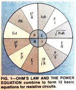
Not to wander off topic, but since the issue of resistor power came up. I thought I would post the power wheel. And maybe for some light comedy relief.

These were popular in workshops , printed on a piece of cardboard hanging on a nail in the workshop in Australia, that is if they had not fallen behind a pile of empty Beer bottles.

(but you can never have too much fun right ?)

The interesting sector is mainly the left upper 90 degree quadrant, the reasons are:

It contains the classic relation that Power = Volts(E) x Amps(I) in Watts. This is why you often see "VA" ratings on appliances which are synonymous with Watts.

And it contains the equation I recommended E^2/R. or V(squared) over R.

The real reason this is helpful, is that in a workshop, the Technician has a voltmeter. Most meters, if there is a pulsitile DC voltage there, just show an average. A smarter meter might show rms, or you might be measuring AC voltage across the resistor.

But the point being, if you take a voltage measurement, across a resistor, you don't have to disconnect anything, and you can usually make a close approximation of the power dissipated in the resistor using this formula.

The other equation (I^2)R or I squared x R, is less helpful, because to measure the current, you have to break the circuit and place the current meter in series.

One of the utilities though, of the (I^2)R equation is in understanding transformers. The (I^2)R power losses are affectionately known as "copper losses" because they relate to the heat generated in the copper wire on account of its resistance R, for some particular rms current I. (the other two losses in transformers are Hysteresis and Eddy current losses relating to the core).

So when somebody talks about "I squared R losses" most of the time, they are talking about losses in copper conductors, and typically in transformers.

You could print out the wheel and hang it on the wall.
 

Attachments

  • power.jpg
    power.jpg
    376.3 KB · Views: 12
Nice addition. As a kid I drew one and pinned it up over my bench. Very handy indeed in my early learning.

And I don't think I've ever seen/heard the word "pulsatile" used in the wild. Props for that.

Now, if more people understood what "pixilated" means, "pixelated" might not have caught on the way it did.
 
Last edited:
Would someone be so kind as to direct me to the schematic for Dwight's 6530/6532 adapter? I'm editing his original instructions on the use of his debug board into something much more usable (and reconciling the discrepancies with the available schematic), and now that I've hit the part about programming the E^2 on these little daughter boards I'd like to make sure I understand the material. Unless I'm misreading things, it's not the same as the Corsham board, is it?
 
As promised, attached is a proper schematic for Brother Dwight's board. Having put some time and effort into it, I think I've earned the right to get up on my soapbox for a moment.

The schematic I worked from was apparently reverse-engineered from a PCB, as Dwight's original drawing was accidentally lost. The recreated schematic was, frankly, a mess - sketchy, inconsistent, and utterly failing to show any kind of rational signal flow. Signals entered in the middle of the drawing and from there went in all directions. Most of the connections weren't drawn at all, instead indicated by tags. The result was that it took an unusual amount of staring at it to figure out what was going on - in a simple circuit that anyone should be able to fully comprehend at a glance. Far from being complete, the information contained therein was so inadequate that to sort it out I had to refer to the original KIM manual, photos of the completed assembly, and stray notes.

I don't entirely blame the person who did it; I've done enough reverse-engineering to know that it's a buttload of work, and the time and difficulty involved are probably an exponential function of the number of components and nets. But if you're not ready, willing, and able to do it right, don't bother. Aside from apparently lacking any sense of what a schematic should look like, said person was further hobbled by the use of KiCAD. Now, I've thought a lot about how best to describe KiCAD's schematic capture, unable to settle on whether it's goat sodomy or a dumpster fire. Upon consideration, though, I realized that such a choice wouldn't at all be fair, because it's actually goat sodomy in a dumpster fire, and about the worst tool I can imagine for reverse-engineering, which inevitably requires repeated rearrangement of the drawing in order to wrestle a random pile of symbols and wires into a rational and comprehensible drawing. This is because its schematic capture has no proper understanding of the actual meaning of connections and nets. When you make what you think is a connection, it really isn't one at all - it's a faux connection, nothing but two coincident points in space that hold no significance whatsoever for KiCAD until some time later when a netlist may be extracted. But it's a recipe for disaster because it doesn't maintain net connectivity, which means it doesn't maintain design integrity. So I'm not just blaming the draughtsman for a bad drawing, because unspeakably poor tools make producing a quality document difficult or impossible even for someone who knows what the finished product should look like. I'm on the record as saying that KiCAD is, overall, an admirable accomplishment, and its layout tools may be first-rate, but I'll never find that out for myself as long as its schematic capture - the design process's front end - isn't fit for polite company or the attention of grownups. When I explain the reality of KiCAD's schematic capture to real live EDA professionals, their jaws drop. Every single time.

Enough of that rant. This how the drawing should look, and it encompasses all of the information needed to construct the circuit. It shows two versions: What I understand to be Dwight's original, based on the above-described recreation; my modified version. Dwight did one thing that I don't like, and that's asking totem-pole TTL outputs to sink current for the LEDs. LSTTL isn't designed to sink more than 8mA, and you can't get much brightness out of most LEDs with that little current - I usually think more along the lines of 20mA. So I replaced his 7404 with a 7405 (and the necessary pullups), and since he had two spare inverters those became my LED drivers. Oh - I also added a power LED. That may seem trivial and unnecessary, but without it this pair of boards can be live on the bench without any visible indication of such.

Hope you find it useful, and if you happen to spot any errors please let me know so I can sort them out.
 

Attachments

  • KIM-1.debug.pdf
    81.5 KB · Views: 14
Last edited:
Much appreciated for the work done. Not being conversant in designing PCBs, I did not know KiCAD was so problematic with schematic capture. I have been trying to learn it to convert old artwork into something modern board houses can use, but I cannot figure out how to trace or do nice curves at all with KiCAD. It feels hopelessly complicated.
 
Perhaps I could offer some guidance if you were to elaborate on what kind of old artwork you're trying to convert, because tracing might not be the right approach and "nice curves" don't mean anything - in this context. I think that might be a little too far OT for this forum, though I'd welcome a PM.

The kind of descriptions that come to mind when talking seriously about KiCAD's schematic capture are "abomination", "war crime", and "Jesus wept". The much bigger problem is that its users actually attempt to defend it with arguments that are far beyond simply irrational and nonsensical. I've been a proponent and supporter of open-source software for decades, but in this case the ignorance of its fanatics really does reveal them to be cult victims.

That aside, though, all EDA feels hopelessly complicated until you understand normal design flow, and then apply those concepts to the particular package you're working with. Some are easier than others; the one I use has a learning curve that lasts for years, but has UI features of staggering brilliance that others can't even imagine - and haven't tried to.
 
Last edited:
Perhaps I could offer some guidance if you were to elaborate on what kind of old artwork you're trying to convert, because tracing might not be the right approach and "nice curves" don't mean anything - in this context. I think that might be a little too far OT for this forum, though I'd welcome a PM.

The kind of descriptions that come to mind when talking seriously about KiCAD's schematic capture are "abomination", "war crime", and "Jesus wept". The much bigger problem is that its users actually attempt to defend it with arguments that are far beyond simply irrational and nonsensical. I've been a proponent and supporter of open-source software for decades, but in this case the ignorance of its fanatics really does reveal them to be cult victims.

That aside, though, all EDA feels hopelessly complicated until you understand normal design flow, and then apply those concepts to the particular package you're working with. Some are easier than others; the one I use has a learning curve that lasts for years, but has UI features of staggering brilliance that others can't even imagine - and haven't tried to.
There are a 1000 ways to make a pcb that will work, but......

The thing is though, if you are interested in vintage computers, how do you create an "exact replica pcb" from a design from the 1970's. By that I mean every track trajectory and curve matches the original ?

It is slightly more difficult than it looks, even with KiCad.

When people realized how collectible and expensive the Apple One computer board was becoming, quickly supposed replicas of the Apple 1 board appeared.

But, the designers messed up the "exact copy".

Tracks had the wrong radius of curvature and trajectories and didn't match up with the original.

In the worst cases, the board didn't match at all because somebody who had a better social life (than staying home in the workshop) refused to burn the "Midnight Oil", and heaven forbid, used a track auto-router where a Chimp could have done a more attractive job of arranging the the physical tracks that conformed to the schematic. I'm afraid this is what you get from every auto router I have seen. The result lacks the elegance of what a concentrating Human mind can create.

I found it was possible to make exact pcb replicas, but the process initially at least, had to be divorced from pcb routing software, and simply use a drawing program to trace over the original pcb track work.

Luckily, in Australia a pcb program in the early days was used called Protel. This evolved into the modern version known as Altium. With this my pcb maker was able to import the images and draw over them, to create exact track replicas for me. This I believe can be done in KiCad too.

Here are some examples: the Dazzler pcb's and for the 4 layer RM-65 video card and many more, including the Votrax Type 'N Talk:

www.worldphaco.com/uploads/THE_WORLD_FAMOUS_CROMEMCO_DAZZLER.pdf


www.worldphaco.com/uploads/THE%20RM65%20CRTC%20MODULE%20AND%20THE%20AIM.pdf


www.worldphaco.com/uploads/VOTRAX_TYPE___TALK_MEETS_HERO_JR.pdf
 
Last edited:
Honestly (and Hugo, I've taken a quick look at some of the stuff you've worked on, and it's interesting, alright... e.g. though I worked at a shop in the late 70s that sold a lot of Cromemco (Z2-D, System 3), I never actually messed with a Dazzler), I don't get this modern repro-mania, especially when it comes to the obsession with slavishly following the radius of a curving trace. It's silly, and possibly unhealthy. It doesn't affect the operation. In one respect it's admirable that you went to all that trouble to clone the original Dazzler layout, but on the other hand, I could probably bang out a functioning copy using slit-n-wrap in an evening with - literally - what I have lying around my lab, just like I didn't have to send out for anything in order to build this KIM diag board. Wait for PCBs to come back from fuggin' China for this? What, like I don't have a matching Vector board and the edge connectors on the shelf? Barmy, mate.

Now, I'm not arguing against doing reproductions - I'm in the middle of a complex multi-board repro project now, but it's for a good reason: It's a tool that performs an uncommon task that is otherwise very hard to either find or accomplish by other means. The available schematics are poor almost to the point of unreadability (hand drawn - not well - and photocopied n generations), and I needed to get an example of the original hardware in order to validate my redrawing (as in the case of this KIM board, only way, way worse). And it's full of obsolete parts too. But I can justify this because it's a tool, not a toy, and I'm making no effort to replicate the traces, because a connection is a connection is a connection.

So here's my proposition: It's not an authentic reproduction if you don't do it the way it was originally done. Turn away from your CAD system and tape it like a man. Blow up those published layouts to 2x and get busy over the mylar on the light table. Forget the Gerbers, we didn't have 'em back then, we used the film we got back from the repro house that shot down our artwork. Generate the drill tape the hard way.

CAD-based repro? Wotta copout.
 
As I stated, I lost some of my original KiCad work when I made mistakes trying to back it up. I'n sorry about that.
And yes, the circuitry I did for the 6530 to 6532 is nothing like the Corsham's or even Ruud's board ( I believe the original design ).
I did a lot of things that were determined by the desire to squeeze all the circuitry under the 6532 chip.
Even things like the assignment the pins on the PAL were determined by how easy it was to route the wiring.
The EEPROM chip was originally a flat pack with the lead splayed out. I folded them under to make the foot print smaller.
Even the EEPROM's data and addresses pins were mixed up and used in "out of order" to meet routing requirements and programming modes.
There were more address pins than were needed for 1K of code so the normal thing would be to tie them high or low.
This would have used up more routing space. Many addresses were simply tied together, keeping in mind the requirement to
to program the parts in the KIM system. The data pins are not in D0 to D7 order either. I doubt you could take a EEPROM
and wire it in the normal order and get it to program with out modifying my programming code to match the address and data order I used.
I also wanted it to be used for -002 or -003 with configuring in the PAL select.
There is another difference and that has to do with the addressing of the I/O of the 6532. I wanted it to be as accurate as
possible for all the possible application of the KIM. Both Ruud's and Corsham's would not do interrupts correctly, if
that was required by the application. I made changes that I believe made it possible to use interrupts.
This meant it would be difficult to address the full additional RAM that the 6532 had compared to the 6530.
Again, a compromise I made to meet the small wiring space.
The original kits, I sent, came with the two small boards that I designed that fit under the 6532. Because of the difficulty in
soldering the EEPROMs, I soldered them in all the kit boards. They still had to be put together with tiny wires bridging some
but not all of the 40 pins. There were a about 40 additional wires there as well, between the two boards.
All this was done, not to make it more complicated to copy or replicate, it was done just to pack all that was needed under the
6532. The instructions to build them described how to put them together. ( not a task for the faint of heart).
As it turned out, I don't believe any of the kits, I sent out, actually built the 6530 to 6532 replacement modules.
The most common failures were on other parts of the board, easily isolated by the diagnostic board tests.
My KIM was damaged by the reverse voltage. It took out both the CPU and the -002.
I recommend you build the diagnostic board first.Then if you find a problem with the 6530 it can be dealt with then.
Dwight
 
Dwight:

Good to hear from you. Please scroll up to posting #166 to find the redrawing of your diagnostic board that I just completed.

I built it and it's working fine on the bench. I'd like to do the same for the 6530/6532 board, so is there any design information I can work from? Or do we have to try to track down one of your kits and do the same reverse-engineering on it? This isn't something I need for myself (that is, afaIk right now, as I've tested one of my KIMs - and it's fine - but not yet the other). I'd like to do it for the community.

Jonathan
 
As for the LED resistor values, I was not trying to light up the room, I just wanted them to light bright enough to be seen.
One doesn't nee to slam them with 20 ma just because they can. You can use whatever current you like.
Dwight
 
As for the LED resistor values, I was not trying to light up the room, I just wanted them to light bright enough to be seen.
One doesn't nee to slam them with 20 ma just because they can. You can use whatever current you like.
Dwight
Sure, but you had the two extra inverters available, so why not do it right?
 
Dwight:

Good to hear from you. Please scroll up to posting #166 to find the redrawing of your diagnostic board that I just completed.

I built it and it's working fine on the bench. I'd like to do the same for the 6530/6532 board, so is there any design information I can work from? Or do we have to try to track down one of your kits and do the same reverse-engineering on it? This isn't something I need for myself (that is, afaIk right now, as I've tested one of my KIMs - and it's fine - but not yet the other). I'd like to do it for the community.

Jonathan
I still have some of the original boards for the 6530/6532 ( rev 1 ) boards. Rev 1 had one small trace missing on one of the boards. I'm not sure if I have any Rev 2s left. I can send them or make top and bottom pictures. If I sent them, I'd like them back after they were copied.
The picture on this thread of one working has the wire missed jumped. I think I still have the PAL file as well.
Dwight
Sure, I'd be happy to do it and the boards will return to you. PM me and we can exchange contact info, addresses, etc.
 
Sure, but you had the two extra inverters available, so why not do it right?
It was more about getting it to work. It was also the first board I did using KiCad. I had enough troubles getting the tool to do what I wanted it to do, never having used a CAD tool before in my life. I've since used it for my 4004 recreation. I had to make all my own 7400 package because I needed to cut cost of the board ( still made mistakes ).
Dwight
 
Hey, if it works for you and makes things easier then I say go for it. Plus you learn about laying out PCBs which I have never tried. What does it do? Maybe others could use this? You have the required cup of tea, so you started on the right foot. :)
 
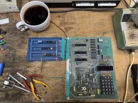
What does it do? Maybe others could use this?

What thread are you in? What conversation did you just enter? What is the context?

Scroll up a few postings and you'll find the schematic and all will be revealed.

My point is that cheap Chinesium PCBs have made people spoiled and many haven't learned (or have forgotten) that if you just need to wire up a simple circuit for your own use and aren't going into production you don't need a PC board. Keep a well-stocked junk box and your wits about you and won't have to spend any money or wait for the board turnaround.
 
Back
Top