• Please review our updated Terms and Rules here

Project to create an ATX 80286 mainboard based on the IBM 5170

At some point I may look into this in more detail after some other things are progressing after the delays caused by getting U87 right.

I think when you wire an output back to another input, the minimization methods could possibly eliminate it altogether because they only observe the output state at one moment, and not the result of outputs changing state.

I think those methods are not able to catch that kind of logic but rather only do straight reads of inputs and outputs.
Probably half of the logic required could be visible after knowing how it was done. I made a gate representation from Logic Friday of what PA.EXE could produce, it's in the attachment. Probably some feedbacks should complete a form of latch circuit.
Instead the equations from PA.EXE to the unconnected pins lead into output pins which are not connected to anything, which can't be right, IBM would never do that for no reason. The feedback is inside the PAL.

I could try the whole approach in another way which I think has more chance of detecting it, by wiring U130 to a test circuit and simulating the signals with switches and LEDs, and the behaviour should be observable like it's described. That would be another confirmation which might be easier, maybe I will make a wired PCB and do that later.

I really want to get a working system together first, and I will have time to look at testing the coprocessor more after other things are done.
 

Attachments

  • U130_logic.png
    U130_logic.png
    7.9 KB · Views: 4
I have decided that I will not be testing any memory modifications on the 5170 first, today I have started the work to go straight to a new prototype design for the 80286 mainboard PCB.

I have weighed the risks because the modifications needed on the 5170 would be extensive. And the 5170 in its basic form is rather limited, not even having the full 640kb of RAM and no UMB RAM either. Certain games I can't even test because of my 5170 not having enough RAM.

Modifying the 5170 would be a lot of work of desoldering, wiring, verification with schematics, manufacturing an ISA PCB, etc.
And the result will be a "test setup" which I will later disassemble again.
My goal is not to reproduce the 5170, however I do aim to reproduce the technology of the 5170, which is really what matters to me.

The design goal will be a mainboard which is fully expanded onboard and will require few cards to create a complete PC.
If anyone has some suggestions of nice open source hardware which would benefit my project, please let me know about it, since right now I am doing the first revision design to assemble everything.

I will be spending all my spare time on creating the new design instead and no more testing. I will do a lot of preparation and verifications of all the logic areas and modifications involved instead, as I have done with the XT design before.

All decoder circuits and databus conversion control will be done in CPLD using one or more through-hole PLCC sockets with programming headers because this requires a lot of logic circuits, especially when creating the decoding for example for something like 10 megabytes of 16 bit XMS memory. Using CPLDs will make my work much easier and also benefits the PCB layout.

My plan is to feature a primary and secondary IDE port using the XT-IDE AT compatible BIOS option ROM, simple SCSI and floppy drive controller onboard, as well as a RP2040 controlled USB mouse port according to the USB to serial mouse project I discussed earlier.

For the keyboard I feel it's not that important to have USB support compared to replacing the serial mouse, I may or may not do that.
Otherwise I will be using a PS/2 keyboard connector. I have tested several PS/2 keyboards with the 5170 without any issues.

The featured BIOS will be primarily the MR BIOS generic 286 version. And I will not be doing any turbo switching either and instead feature a fixed clock speed for everything.
If anyone has some ideas about how I could feature a POST display, I would be interested to know more about this in order to possibly integrate it onboard, if there is any open source solution made.
I have not done any research about POST displays yet, I would be looking for something compact and specific for an AT system.
 
As I share the dream of building my own 286/AT machine, I also have some ideas what this machine would look like. Maybe some of my wishes help with your design.

Enclosure:
This is, in my opinion, one of the most neglected topics in many PCB designs. For Raspberry Pi I even did my own carrier board (https://pipci.jeffgeerling.com/boards_cm/johanns_carrier_board.html) as the available PCBs sucked so much when it came to finding an enclosure. And even for my 286/AT, I would love to use such an aluminum slide-in case. On the other hand, for an AT PCB design, ATX is of course a very valid choice, and I'm not suggesting something else.

So, my idea would be to use a 3D printed pizza box like design. Its base would be only minimally larger than the board footprint and aluminum would be used as a base plate just for stability reasons. I would use a pico ATX power supply so no additional enclosure space is required. The height would at most be enough for low profile ISA cards, but I would like to make it even slimmer and maybe use a 90 degrees ISA adapter to mount any ISA card horizontally. Or even better: Use no standard ISA card at all. Instead, could you provide some pin headers for the ISA bus, so that custom extension boards could be used? Maybe in the area where the ATX backplate resides, so that two rows of connectors can be exposed through the ATX backplate? Per my understanding, you could even use PC/104 as a standard way for exposing ISA via pin headers.

Sound card:
This would even provide classic joystick port emulation via USB, matching your mouse approach!
Maybe even on-board? OTOH, SMT would suck...

VGA card:
Sadly, only CGA is available for this board at the moment, and I want VGA.

I really want DVI/HDMI. And I'm even thinking about designed my own VGA card (low profile or PC/104, of course :) ) with a Chips&Technologies ct65545 (or similar). These chips are widely (and cheaply) available still and per my understanding allow a single-chip VGA solution (ok, plus RAM...) with HDMI just requiring an additional TMDS encoder.

Floppy:
Gotek with https://github.com/keirf/flashfloppy

Harddisk:
Compactflash. From my understanding, some CF cards want 3.3V, so making 5V/3.3V on IDE jumper-selectable would be a nice-to-have? Or maybe an CF socket on-board?

THT vs. SMT:
Please stick to THT - it really seems adequate for such a retro board.
 
Last edited:
Since the ISA bus isn't really "smart", couldn't you:
* Put one standard ISA slot on the PCB, ideally in a way that lines up with an ordinary ATX case
* Build a "riser card" that slid into an ISA slot but had three or five more slots on it

I feel like that sort of splits the difference: you can either build the low-profile pizza box style setup, or you can use an off-the-shelf ATX case if you only need one card.

But then you have to ask if one card is going to be viable. If you integrate a VGA chipset and the contents of a typical multi-I/O card (one or two IDE channels, optionally serial/parallel/floppy/game port), then you can have a reasonable build with zero cards and save the slot for stuff like sound or networking. OTOH, if it's functionally the equivalent of a typical 286 baby-AT mainboard (no onboard peripherals), one slot really isn't enough.
 
Thanks HoJoPo,

I like this card, very simple and basic and easy to integrate as an extra feature.

The Faraday A-Tease had an integrated 8 LED DIP display on board for codes.
Hi Chuck, thanks for mentioning this, I will search around to see if I can find an example of what it looks like.

Maybe some of my wishes help with your design.
Indeed it's interesting to read. I love this type of aluminium case design, I should have one somewhere in my old parts boxes that I never used.

I constructed a 19 inch frame design Z80 computer long ago but at the time I didn't have much system design experience and it was highly unstable.
Since then I did a Z80 ATX mainboard recently which has a lot of stuff onboard and CP/M.
That system is really suitable for a modular construction however my design featured a multi bus approach because I wanted to construct a Z80 version of a PC.
Actually that project led me to building an XT just to get more experience.
Once I built an XT, I got kind of hooked by nostalgia of the DOS days and stuck with those types of designs.

A while ago I also searched for a modern VGA card recreation but I also never found anything.
I mean, besides using new old stock and recycled known VGA ICs.
And those are usually extremely pricy which makes buying a used old card a better option.
Same thing for sound cards, except for the PicoGUS. I do like this concept though, I am not sure if the creator would agree me to integrate one, it seems he is selling them also to fund his development and testing work, which I don't want to interfere with his process.
Is this card able to work for DOS games instead of a Soundblaster?
From the compatibility list it seems not transparent, I should try to build this and test it out just to see if it's interesting for me to use this card.
Anyway, I'm not looking to integrate sound or VGA, though sound is more interesting. I feel this is really something that should remain optional.
Though I do feel it would be great to build recreations.

I mean, I could reproduce some old design using the 6845 but those are very limited in specifications of course.
Though it may be fun to try some old games on them which were rewritten from source to support CGA or similar old graphics cards.
I only own a ATI Small Wonder 2 card which is nice because it can output composite video.
I have some old CRT screens and modified a small monochrome Philips TX TV to remove all the TV stuff and only keep the video section.
It's nice to see DOS on a TV.

I do appreciate the FPGA reproduction because this can replace the CRT controller chip which will become more and more rare over time.
So there is a degree of preservation done by creating these cards, which is a good thing.
I hope that more ICs of the core logic of PCs could be reproduced and in FPGA.
Such as the 8237, 8259 and 8254 etc.
The concept of FPGA reproduction is really useful so the full design of PCs can be preserved and reproducable in the future.
This may also appeal to students as a project to work on, and can let more people know the history of PC technology.
It is the same what I am trying to do, except one step further.
I do have such plans for the future to look more into this.

If only there were a good VGA adapter recreated in FPGA, I would look into integrating it onboard since it would be adequate to use one.
A single PCB which includes everything is also an option to build into a ATX housing. The slot positions may be used to put connector brackets there.
That is also a path, however VGA was never done adequately to replace that. I think the development would be really difficult because of requiring a BIOS software to be developed.
That is a more involved process for sure.
I am facing the same problem with my Z80 PC. It needs a good VGA capable design, since I now only have a TI CRT controller with limited resolution available to be used with CP/M.

About floppy and harddisk, I really love something close to original hardware, what I am using for my retro designs are mechanical laptop IDE harddisks.
And I simply love the old floppy drives as well. It's fun to hear the floppy drive seeking and stepping through a disk.
XT-IDE BIOS is really great to be able to control larger harddisks.

I wish someone could create a project to replace or modify the drive electronics on a SATA harddisk so it can function with an IDE interface.
I have tried those converters from SATA to IDE but they were not able to function on the XT-IDE, it's probably only compatible with modern BIOS software.

About through-hole technology, this is also my preference however some things are not found in through hole versions, such as the Realtek LAN chip and SCSI adapter ICs.

When using CPLDs I will try to keep PLCC and through hole sockets if possible. On the other hand, when using a good flux, soldering SMD is really not that hard to do, and hot air soldering equipment is really cheap now. It all comes down to the technique, and can be a fun experience to learn. I used to repair a lot of SMD equipment in the early 2000s. Some ICs simply will have larger size and will need at least PLCC sockets in this generation of PC technology. After reverse engineering U87, I have realised it's no longer feasible to maintain a DIP-only design. So I will move on the use CPLD more extensively because this will benefit the level of onboard integration which has always been my goal to maximize this. On my first XT I integrated only a few things, but this time I will go straight for maximum integration on the PCB.

Regarding the format of the PCB, there is really no option to realistically do this in any other format than full size ATX. It would not make sense to create a different or new format PCB because that would create all sorts of problems to find a suitable housing. The industry already created various solutions which make building a PC much less involved. I mean, if there were another format of cases widely produced which also supports adding a mechanical hard drive, CD-ROM and 3,5 inch and 5,25 inch floppy drives, I would love to consider it, however the manufacturers are making only limited models of cases today which still support this. In fact, I am happy they still do since these days building a PC often doesn't include any separate drive devices, instead only a few SSD cards plugged directly into the mainboard instead. So the future of PC case development seems also uncertain. Maybe one day there will be limited options which will motivate people to make their own formats.

Actually, my preferred PC case is still the original IBM cases, however those are even harder to obtain and super expensive. I also love the clone 286 desktop format cases as well. some of those look really good. But those are also often sold for high prices. I recently bought a IBM 5150 case from Ebay. I am also doing a new 5150 design because I want to include tape storage. I will create a board that fits this case, however on a ATX power supply principle. I plan to buy a IBM power supply and replace the electronics with a really good ATX PSU. I want to make a fun front panel with LEDs and tape data information in one of the 5,25 drive mounting places. Since the mainboard will also be integrated, this case having 5 slot positions is really fine for my purpose.

I also love the pizza box format most Hak Foo, and I don't think an ATX board would persé be limited to only be used in a ATX case, I think it should be possible to modify it to fit a pizza box. Unfortunately those are not very standard, otherwise that would really be my preference to design for one! Regarding the ISA slots, a builder can easily leave out the slot connectors and only solder one in a corner. Then only a simple PCB design would be needed to provide horizontal mounting. I definately want to do such a project at one time. I could design a board to accommodate such a case however I don't have a reference case for this. Not having such a case it's hard to make sure things will fit, and also it's no motivation for me to do this work. A pizza box case is really great, just design a large PCB on the bottom is also cool to do and really supports even more integration. Maybe I will come across a widely used pizza box case, if I can buy one that would incline me more to do such a design. I had a old HP Compaq tower/desktop case and removed the mainboard and modified the case to mount a ASUS P4B533 mainboard, which is reasonably suitable for retro software purposes. My point is, modifying a case is definately also an option to get the kind of build that you want. If you have ideas about what kind of case you like, feel free to post photos here of what you like, it may give me some ideas for the future. For example, I also like the IBM PS/2 cases, and I love the old Tulip pizza box PC designs, I have some nostalgic memories of my school days, working on them with CAD software.
 
Last edited:
I forgot to mention, integrating a CGA or monochrome display adapter onboard is something I may be interested in if space permits. Since these adapters are BIOS supported to generate the display from the system BIOS, it can be used side by side with a VGA card, it may simply be a cool addition to the design, allowing to plug a composite CRT optionally.
 
Even though PA.EXE turned out to work fine, I decided to finalize pa.py, so that it also provides OE equations. Maybe this is useful for future PAL analysis.
 

Attachments

  • pa.zip
    2.6 KB · Views: 2
Thank you Johann for taking time to finish this,
I saved the new script for future use.

It's certainly helpful to have more options.
Also your address to logic conversion script was super helpful.

I still have a Super Nintendo copy box full of GALs that I may want to reverse engineer some day.
I did some work on it before but my logic analyser appeared not to be reliable enough.
It's based on DRAM so a lot of stuff will not be needed anymore.
Maybe the remaining logic will turn out to be more simple and straight forward, quite possibly so.
I simply liked the idea of expanding a Super Nintendo into a whole system.

I think I have a multi I/O card somewhere with a GAL on it, could be interesting to look at this also.
 
Rodney, could you provide the “eprom dump“ for U130? Then I would have a second sample for verification of pa.py.
 
Sure Johann, please see the attachment.
 

Attachments

  • MacDonald_Read_27C020_U130.zip
    2.6 KB · Views: 3
Out of curiosity, I checked if I could not also simplify the terms in Python. And with "sympy" it was surprisingly easy.

I got:
~END_CYC = Q4
| AIOW & ~RES_0WS
| RAS & ~RES_0WS
| FSYS_16 & Q1 & RAS
| AIOW & Q1 & ~IO_CS_16
| Q1 & ~IOR & ~IO_CS_16
DMA_AEN = AEN_1 & AEN_2
XA0 = 0
XBHE = AEN_2 & ~AEN_1 & ~XA0
~GATE_245 = FSYS_16 & RAS & XA0 & ~AEN_1
| FSYS_16 & RAS & ~AEN_1 & ~AEN_2
| FSYS_16 & XA0 & ~AEN_1 & ~IOR
| FSYS_16 & ~AEN_1 & ~AEN_2 & ~IOR
| AEN_1 & AEN_2 & AIOW & IO_CS_16 & XA0 & ~XBHE
| AEN_1 & AEN_2 & IO_CS_16 & XA0 & ~IOR & ~XBHE
| AEN_1 & AEN_2 & RAS & XA0 & ~FSYS_16 & ~XBHE
| AEN_1 & AEN_2 & XA0 & ~FSYS_16 & ~MEMW & ~XBHE
~DIR_245 = MEMW & RAS & ~AEN_1
| AEN_1 & AEN_2 & AIOW & ~XBHE
| AEN_1 & AEN_2 & ~MEMW & ~XBHE
~DATA_CONV = AEN_1 & AEN_2 & AIOW & IO_CS_16 & Q1 & ~XA0 & ~XBHE
| AEN_1 & AEN_2 & IO_CS_16 & Q1 & ~IOR & ~XA0 & ~XBHE
| AEN_1 & AEN_2 & Q1 & RAS & ~FSYS_16 & ~XA0 & ~XBHE
XA0.OE = ~AEN_2
XBHE.OE = ~AEN_1
| ~AEN_2

With the exception of ~GATE_245, these equations seem to match Rodneys. I will check this one difference when I find time.

I also renamed the script from "pa" to "pete" - PAL epromdata to equations (;)) - source attached.

Cheers,
Johann
 

Attachments

  • pete.zip
    3.8 KB · Views: 2
Hi Johann,

It's amazing you have come very far with your scipt, my compliments!
And let's not forget that your script is a one-step solution, including to do the work of Logic Friday as well.
That saves a lot more time in the reverse engineering process.
I was initially not even able to find concise clear instructions that I should use Logic Friday or similar after obtaining the PA.EXE output.
So your script is potentially able to save a lot of time and work!

It would be really great if you could arrive at the same results as mine in a single analysis, which would definitely validate the script in the use case example of U87.

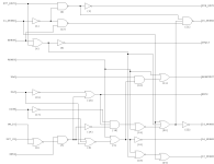
I have done a careful compare for the terms in your output.

Code:
~END_CYC = Q4
  # Q4;
| AIOW & ~RES_0WS
  # AIOW & !RES_0WS
| RAS & ~RES_0WS
  # RAS & !RES_0WS
| FSYS_16 & Q1 & RAS
    FSYS_16 & Q1 & RAS
| AIOW & Q1 & ~IO_CS_16
  # AIOW & !IO_CS_16 & Q1
| Q1 & ~IOR & ~IO_CS_16
  # !IOR & !IO_CS_16 & Q1

DMA_AEN = AEN_1 & AEN_2
DMA_AEN = AEN_1 & AEN_2;

XA0 = 0
XA0 = 'b'0;

XA0.OE = ~AEN_2
 XA0.oe     = !AEN_2;

XBHE.OE = ~AEN_1 | ~AEN_2
!XBHE.oe    =  DMA_AEN;

(no value from your script)
RES_0WS.oe = 'b'0;

XBHE = AEN_2 & ~AEN_1  & ~XA0
XBHE =  AEN_2     & !XA0;

~GATE_245 =
    FSYS_16 & RAS & XA0 & ~AEN_1
  # !AEN_1 & FSYS_16 & RAS & XA0
| FSYS_16 & RAS & ~AEN_1 & ~AEN_2
  # !AEN_1 & !AEN_2 & FSYS_16 & RAS
| FSYS_16 & XA0 & ~AEN_1 & ~IOR
  # !AEN_1 & FSYS_16 & !IOR & XA0;
| FSYS_16 & ~AEN_1 & ~AEN_2 & ~IOR
  # !AEN_1 & !AEN_2 & FSYS_16 & !IOR
| AEN_1 & AEN_2 & AIOW & IO_CS_16 & XA0 & ~XBHE
    AEN_1 & AEN_2 & AIOW & IO_CS_16 & XA0 & !XBHE
| AEN_1 & AEN_2 & IO_CS_16 & XA0 & ~IOR & ~XBHE
  # AEN_1 & AEN_2 & !IOR & IO_CS_16 & XA0 & !XBHE
| AEN_1 & AEN_2 & RAS & XA0 & ~FSYS_16 & ~XBHE
  # AEN_1 & AEN_2 & !FSYS_16 & RAS & XA0 & !XBHE
| AEN_1 & AEN_2 & XA0 & ~FSYS_16 & ~MEMW & ~XBHE

~DIR_245 = MEMW & RAS & ~AEN_1
    !AEN_1 & MEMW & RAS
| AEN_1 & AEN_2 & AIOW & ~XBHE
  # AEN_1 & AEN_2 & AIOW & !XBHE;
| AEN_1 & AEN_2 & ~MEMW & ~XBHE
  # AEN_1 & AEN_2 & !MEMW & !XBHE

~DATA_CONV = AEN_1 & AEN_2 & AIOW & IO_CS_16 & Q1 & ~XA0 & ~XBHE
  # AEN_1 & AEN_2 & AIOW & IO_CS_16 & Q1 & !XA0 & !XBHE;
| AEN_1 & AEN_2 & IO_CS_16 & Q1 & ~IOR & ~XA0 & ~XBHE
  # AEN_1 & AEN_2 & !IOR & IO_CS_16 & Q1 & !XA0 & !XBHE
| AEN_1 & AEN_2 & Q1 & RAS & ~FSYS_16 & ~XA0 & ~XBHE
    AEN_1 & AEN_2 & !FSYS_16 & Q1 & RAS & !XA0 & !XBHE


There are a few things which stand out, one of which I think can be easily solved with a small addition, so let's start with this one:
RES_0WS.oe = 'b'0;

Any input/output pin which is used exclusively as an input, and not switching to being an output under any circumstance, not having any OE equation, should have the OE function permanently disabled.
So if there is no value for PIN.oe determined by the analysis, and it's not appearing as an output in the analysis, in other words, if PIN appears as an input pin, having no OE function, the script should state the PIN.oe value to be 'b'0. It's important to state this to WinCupl otherwise it may assume wrongly that PIN.oe equals 'b'1. Maybe this is some kind of bug or something I am not seeing why WinCupl does this, so the safe path would be the above stating of PIN.oe = 'b'0 by the script.

Using Logic Friday for !GATE_245 -only-, I was getting
Minimized:
GATE_245 =
RAS AEN_1' AEN_2' FSYS_16
+ IOR' AEN_1' AEN_2' FSYS_16
+ RAS AEN_1' FSYS_16 XA0
+ IOR' AEN_1' FSYS_16 XA0
+ IOR' IO_CS_16 AEN_1 AEN_2 XA0 XBHE'
+ AIOW IO_CS_16 AEN_1 AEN_2 XA0 XBHE'
+ RAS AEN_1 AEN_2 FSYS_16' XA0 XBHE'
+ MEMW' AEN_1 AEN_2 FSYS_16' XA0 XBHE'

The last term here can be reduced by the following reasoning:
RAS from the circuit diagram of the 5170 is a positive logic combination of !MEMW and !MEMR.
!RAS = !MEMW & !MEMR
Which means that RAS is positive logic true if !MEMW is negative logic true OR !MEMR is negative logic true.
So from this, being an OR function, it could be reasoned that
+ MEMW' AEN_1 AEN_2 FSYS_16' XA0 XBHE'
is covered by
+ RAS AEN_1 AEN_2 FSYS_16' XA0 XBHE'
and thus the term with !MEMW can be removed from the product terms by reasoning only of the person looking at the matter.
Of course, in this case, both PA.EXE and your script resulted in the same terms so no difference here.

The number of product terms per output which can be compiled in WinCupl is a maximum of 7 AND-OR terms.
Having more terms is technically not an error, only a problem for the person trying to make a functional GAL. ;)

XBHE.OE = ~AEN_1 | ~AEN_2
!XBHE.oe = DMA_AEN;
Here we see that by rewriting
XBHE.OE = !AEN_1 + !AEN_2
-> !XBHE.OE = AEN_1 & AEN_2
-> !XBHE.OE = DMA_AEN
Which is using output DMA_AEN as the inverse OE function, which WinCupl only seemed to be willing to accept for achieving a successful compile.

I have done a final evaluation of my work to see where the problem was created. The biggest problem during my testing work was that I was thrown off by the fact that XA0 and XBHE were being used as both an input and output. Which at first appeared to be impossible and conflicting information, leading me to dismiss it at first, however looking at it again later, it made sense after all because during DMA the CPU is inactive, leaving XA0 and XBHE as tri-state.

That was the seemingly smallest thing which turned out to be the biggest problem in testing.
None of the test GALs could function if the XA0 and XBHE output and .oe functions were not present because these prevented DMA from functioning at all.
So this point was preventing any of my tests with the GAL to work at all, resulting in a totally "dead" 5170 when testing.
Only when connecting U87 and my GAL to the same inputs, by coincidence, I finally discovered the real problem with XA0 and XBHE because having U87 connected with none of the 5 outputs wired to the 5170, I was getting a functional mainboard. That was the final clue that something strange must be going on with one of the inputs being an output in certain conditions.

And these missing output and OE equations for XA0 and XBHE resulted in the deviating results with the EPROM compare reads as well.
Which I then attempted to explain with your other script into additional output terms for !GATE_245 for those reads.
I then reduced these away with reasoning those additional output terms to be covered by a few other existing equations.

So that was a seeming contradiction as well, for which the real explanation were of course the output and .oe terms for XBHE and XA0.
So here also my total lack of PAL reverse engineering experience, which I readily admit, literally it was my first time, played a big role to let me doubt the information from PA.EXE at first. I also had not done any work with PA.EXE before and was yet to gain confidence in it in my personal practical experience. A few times I had the thought that I should contact someone with more experience to discuss the problem. Maybe that would have saved me a lot of time.

One final difference I noticed is this:
your python script outputs:
XBHE = AEN_2 & ~AEN_1 & ~XA0

PA.EXE outputs:
XBHE = AEN_2 & !XA0;

I am wondering how this different answer can appear, I can't explain it and it must be some difference in the software.

I can't by any reasoning assume that the AND term ~AEN_1 can be excluded to be always valid.
So it's unclear to me.

PA.EXE outputs literally:

!XBHE = !AEN_2 & !XA0
# !AEN_2 & XA0
# AEN_2 & XA0;
Where !AEN_1 is eliminated by PA.EXE and not appearing at all.
If you could find this problem that would be really great Johann!

And a small thing, would it be possible to rewrite the outputs using "#" or even "+" instead of "|", and using "!" instead of "~" ?
If possible, that would look even better!

Anyway, I must pay you a big compliment Johann, your python skill in this practical application is impressive!

And I just want to say it clearly once more, my only concern, in both my work and this thread, is to fully preserve and recreate the 5170 in my own modern recreation.
I was totally surprised to find that there was no definitive logic for U87 available on the entire internet.
This matter has cost me around three weeks of time in total.
But the value I did get out of it was a gain of experience that I developed from it.

Which arguably is another reason for me to do these projects, other than it being simply cool! :)

I feel sorry for the IBM team that they were not credited so much for their amazing work on the 5170 after getting famous for creating the PC and XT models. I mean, the 5170 was really a big milestone and iconic! Their "secret sauce"-alike solutions for true 8 bit software and hardware compatibility was absolutely genius and elemental in pushing the industry standard of PCs forward into 16 bit technology in a totally acceptable and "painless" way for anyone looking at the new technology! This point deserves proper credit and should never be overlooked!

When I search for the 5170 development, I hardly see the names of Bill Lowe and Don Estridge mentioned at all. If anyone here reading this knows of a documentary or any other material about the 5170 project, I would really appreciate a mention here! I am really interested in the historical aspect as well, not only the technology.
 
Last edited:
I'm usually just coming directly to the technical stuff, but I'll make an exception here: Please allow me to say how much I'm enjoying our discussion here. It's surely not the first time I'm taking part in an Internet based joint effort, but this one feels special. I mean we met here more or less coincidently and yet it feels like we are instantly acting like a well-established team. What a striking experience!

I also think it makes sense that we use my equations to double check the correctness of yours. My perception is you are taking the way of an electrical engineer and I'm the one of a computer scientist (which I actually am, even I have a strong tendency to get my fingers dirty in electrical engineering stuff). In the end, we should come to the same result. You probably will accept the correctness when it is working in an 5170 board and your own board. I will only accept the correctness, if the "EPROM readout" of the GAL will be identical to the PAL's :) .

Regarding the difference in equations I have two main ideas:
- This "tri-state" stuff doesn't directly fit boolean logic. But maybe it's not so hard to get around this: I can pass "don't care" terms to sympy - and that is probably what "OE disabled" means.
- As we know now (thanks to your hard fight..) XBHE acts as output and input. And, GATE_245 depends on XBHE, which itself depends on other pins. This transitive dependency might be the key to simplify the GATE_245 terms. But I have no idea yet how to teach this fact to sympy...

BTW, I will try to make the not/and/or operators configurable. I just switched to ~/|/& because this is what sympy uses.

I'm also thinking about generating the fuse map directly, making pete.py a single-script solution for converting the "EPROM dump" to a jedec file. Can somebody please help me with the data sheet specification?

1706211009083.png

1. Am I right that this is what's actually limiting the PIN output logic to a sum of at most 7 products?
2. Am I right that the right-most inverter requires me to make to write down the PIN output logic as "Not", i.e. "~Pin1 = Pin2 & Pin3", rather than "Pin1 = Pin2 & Pin3"?
3. Am I right that this limits the PIN OE logic to only a single product?
4. Am I right that the fuse map is just an array of bits where "1" at a certain crossing makes the related input pin part of the product specification for the output pin?

1: Yes, only 7 ANDs feed into the OR, so you only get seven terms... unless you use another I/O pin's feedback to stack another seven terms on. Although technically you can *kind* of use OE as an 8th product by putting an explicit pull-up or pull-down on the output so the OE equation will result in a specific state instead of (effectively) a "don't care". (When interfaced to TTL logic an OE without anything else on the output pin to drive it will *probably* float high, but it's not a reliable given.)

2: FWIW, Most of the languages for expressing PAL equations, like PALASM, will abstract this by letting you put the negation on either the product terms or the pin specification; IE, you can say:
Code:
PIN = /A & B

#OR

/PIN = A & /B

3: Yes, although, again, you could put more products on another I/O pin and drive the OE product with the feedback from that pin.

4: Yes. You'll notice those schematics look a little weird because the ANDs on the product terms only have one input. Wikipedia has a pretty good diagram that will help understand what it looks like in the actual device:
640px-Programmable_Logic_Device.svg.png

Every input pin is duplicated so its actual input value and its complement are connected to the grid as open collector (IE, they can only pull down, not up) logic, and the input pins on the product AND gates are connected to pull ups, which means they'll automatically be a "1" if the fuse connecting them to the grid is cut. At programming time *all* the fuses on the PAL get blown except for the ones that matter for each product, IE, either the inverted or non-inverted connection is left whole so the corresponding input pin can pull it down. (IE, the programming process cuts all the fuses to input pins that are "don't care", and just leaves the bitmap of conditions for each pin you *do* care about.)

The only thing I'll add here is the diagram fragment you snipped did leave out the feedback, which is important. On the particular PAL in question you don't have feedback on the top and bottom pins on the output side, meaning they can *only* be outputs. The other pins look like this:

Screenshot 2024-01-25 at 11.40.09 AM.png

IE, there's that wire coming back into the grid (with both its "normal" and "negated" condition available) from beyond that output inverter that's controlled by the OE line. This is what both allows you to stack additional product terms on another output pin (*note, critically, that this other output pin will need to be OE for its terms to feed back in), and lets you use that pin as an input. If you're *always* just going to use it as an input (IE, you specify it as such in your programming solution by *not* explicitly giving any output solutions) you blow a special fuse configuration that ensures that the OE equation will always be false, while if you're going to do fun tricks like using it bidirectionally, IE, under some conditions assert your own value onto it while other times tri-state it and use the value something else is asserting on it, you'll need your OE value for that pin centered around knowing when it should be talking vs. listening. Typically you'd do this by including as the input equation for OE a signal related to the chip select/OE conditions of whatever other party can assert things on that line.

(That thing I mentioned in reply #1 about using OE as an 8th term if there *isn't* something else on the line is kind of a special case of this, in which you create a synthetic default condition on that output with a pullup/down resistor for the non-OE state.)

Edit: * per the comment about needing to have OE enabled for feedback to work, this is why I was saying earlier that if there were some kind of latching implemented in a combinatory-only PAL like a 16L8 you'd be able to "see" it, because any kind of latch is going to need the feedback to the grid to function, and you're not going to see it on the grid unless it also shows up on the external pin. This of course is not true on a "registered" PAL, because it explicitly has buried latches you can't see, and is why they're such a headache even compared to what's going on in this thread to reverse engineer.
 
Last edited:
Please allow me to say how much I'm enjoying our discussion here. It's surely not the first time I'm taking part in an Internet based joint effort, but this one feels special. I mean we met here more or less coincidently and yet it feels like we are instantly acting like a well-established team.
Indeed Johann, when you joined the thread I had a feeling right away that your assistance and programming expertise could potentially become a big help at some point. And it's great to know you are also looking forward to the final 286 mainboard design a lot and even are interested in building one. I will possibly be doing more than one revision, though I am not excluding that it could be finished as envisioned in a single go. This is also up to my extreme double checking, which I always do in mainboard projects, and a little bit up to good luck that no bug or problem will be present.

Having a common purpose is always very supportive especially in this kind of elaborate project. For processing large amounts of data it has been really useful to have had your programming skills available at those times. I could not move past those strange results by manual composition of all the product terms. Getting insight into those was really elemental for me to move past the compare results and pinpoint the actual problem. I'm grateful you stepped in and impressed how you were able to come to this professional level of logic decoding at such a short period of time! And what an idea to use python to generate the fuse map as well! It's also my pleasure to work with you here. I will be careful to describe all my design steps and points involved here, and if there is any possibility or idea you see it's very welcome to discuss it here. I really appreciate the help and understand the power of python to contribute here and potentially even in other steps. Getting U87 working is a big step forward, possibly even the most important one in the whole project. You know, having the 5170 schematic means nothing without also having the PAL logic inside U87.

I will see about reading the GAL back, great idea! Having more verifications also can give me more peace of mind so I am totally seeing your point.

I will also be working on decoding PROM U115, a 82S123 used for I/O decoding, though this will be a more straightforward matter for the most part I expect. I will be doing some IO reads of this PROM which will result in a binary file for the outputs similar to the PAL reads but much less complex since the outputs are really only outputs. Most of the outputs I could even reason the probable logic for them, however I will do the extra work of decoding it anyway just for the sake of extra checking to make sure.

I will post more information as soon as I have more time later. I am also still looking into the choice of what PC case to use for the new mainboard design.
 

Attachments

  • U115_pinout.png
    U115_pinout.png
    13.4 KB · Views: 1
because it explicitly has buried latches you can't see, and is why they're such a headache even compared to what's going on in this thread to reverse engineer.
Indeed Eudimorphodon, registered logic looks like a big nightmare and I am relieved that IBM didn't use actual GALs or even PAL "R" types.
Thanks for providing the clear explanations, that's really helpful to have that additional clarity about the PALs. The more you look at them, the more it's obvious that even with PAL chips the operations could become more complex if the designer had such elaborate and "clever" ideas for example with the OE functions. The more I thought about it, the more I realized that this had the potential to greatly complicate getting the actual equations finally. Luckily it was not that bad in the case of U87 in the end as it has turned out. I will be doing a readout of the GAL as Johann suggested which is an excellent idea. If any differences turn up, we can discuss it here and possibly get an even more exact match worked out, which is of course also definitely going to help the project.
 
Back
Top