| VCF West | Aug 01 - 02 2025, | CHM, Mountain View, CA |
| VCF Midwest | Sep 13 - 14 2025, | Schaumburg, IL |
| VCF Montreal | Jan 24 - 25, 2026, | RMC Saint Jean, Montreal, Canada |
| VCF SoCal | Feb 14 - 15, 2026, | Hotel Fera, Orange CA |
| VCF Southwest | May 29 - 31, 2026, | Westin Dallas Fort Worth Airport |
| VCF Southeast | June, 2026 | Atlanta, GA |
-
Please review our updated Terms and Rules here
- Forums
- Companies
- IBM Computers, PCs, Clones and Descendants
- PCs and Clones (XT and early AT class machines)
You are using an out of date browser. It may not display this or other websites correctly.
You should upgrade or use an alternative browser.
You should upgrade or use an alternative browser.
Project to create an ATX 80286 mainboard based on the IBM 5170
- Thread starter rodney
- Start date
")
Eudimorphodon
Veteran Member
Is it electrically assured that the PAL drives its outputs in a way which "overrides" what is applied from the EPROM adapter??
Yes. Or, at least, if a PAL’s output can’t overcome a 4.7k resistor it’s probably not healthy. Assuming I’m doing the math right based on the numbers in the datasheet a PAL should be able to overcome a 1K-ish pull-down or a 350-ish ohm pull-up.
Indeed, I am still working on it Johann.Then I keep the fingers crossed you find out the OE equations.
I have done more analysis of which situations the equations for !GATE_245 represent.
Some things in the equations are unclear because more inputs are used than actually necessary.
For example when XA0 = 1, there is no need to evaluate XBHE since there is only one possibility, the high byte transfer mode of the CPU.
Since XA0=1 and XBHE=1 is a situation which does not occur according to Intel, when XA0=1 it's irrelevant what the state of XBHE is.
I have tested several combinations which I suspected to possibly represent floating conditions because of differing reads with pull up and pull down on GATE_245.
However I am not able to change the output logic state in any of those combinations.
So the whole theory about tri-state output conditions is so far not proven yet.
Though the idea is interesting, however I have not seen the proof by being able to pull the output up or down at any of the differing conditions.
I am starting to have less faith in the EPROM reader being suitable for this analysis.
I can't exclude that some readings may be marginal and not clear enough.
It is still strange that the anomalies are consistent.
I don't have any clear and proven explanation for this.
I should get more certainty and I need to find other methods of reading the data from the PAL.
I have some breakthrough news!
Apparently my GAL logic is working after all now!
I discovered today that my test GAL was partially defective, and this was causing it to be unable to properly control the 5170!
This screwed up all my previous tests of the past week.
After programming a new GAL which I took from some PCB, I started testing and each pin I tested turned out to be fully functional.
It is now controlling the conversion on my 5170 completely on its own!
Only for the time being I have !DMA_AEN on the original PAL because the logic doesn't fit(yet).
Next I will do some experimentation to see how I can simplify the equations for GATE_245.
If I can get this done, the whole GAL can replace U87.
Even if that can't happen, my only concern is that the 5170 can function with the GAL logic.
Here is the complete logic, including the adaptations for the outputs to become inputs:
I will update further, I have some theories for simplification of GATE_245 which I need to work out and test.
Apparently my GAL logic is working after all now!
I discovered today that my test GAL was partially defective, and this was causing it to be unable to properly control the 5170!
This screwed up all my previous tests of the past week.
After programming a new GAL which I took from some PCB, I started testing and each pin I tested turned out to be fully functional.
It is now controlling the conversion on my 5170 completely on its own!
Only for the time being I have !DMA_AEN on the original PAL because the logic doesn't fit(yet).
Next I will do some experimentation to see how I can simplify the equations for GATE_245.
If I can get this done, the whole GAL can replace U87.
Even if that can't happen, my only concern is that the 5170 can function with the GAL logic.
Here is the complete logic, including the adaptations for the outputs to become inputs:
Code:
Name     IBM-5170-U87 ;
PartNo   00 ;
Date     13-01-2023 ;
Revision 03 ;
Designer Rodney ;
Company  - ;
Assembly None ;
Location None ;
Device   G16V8A;

/* *************** INPUT PINS *********************/
PIN 15=XA0;
PIN 16=XBHE;
PIN 1=RAS;
PIN 2=MEMW;
PIN 3=IOR;
PIN 4=AIOW;
PIN 5=Q1;
PIN 6=IO_CS_16;
PIN 7=AEN_1;
PIN 8=AEN_2;
PIN 9=Q4;
PIN 11=FSYS_16;
PIN 13=RES_0WS;

/* *************** OUTPUT PINS *********************/
PIN 12=END_CYC;
PIN 14=NUMBER14;
PIN 17=GATE_245;
PIN 18=DIR_245;
PIN 19=DATA_CONV;

XA0.oe = 'b'0;
XBHE.oe = 'b'0;
RES_0WS.oe = 'b'0;

DMA_AEN = AEN_1 & AEN_2;

!END_CYC =
    FSYS_16 & Q1 & RAS
  # !IOR & !IO_CS_16 & Q1
  # AIOW & !IO_CS_16 & Q1
  # RAS & !RES_0WS
  # AIOW & !RES_0WS
  # Q4;

NUMBER14 =
    AEN_1 & AEN_2 & !FSYS_16 & RAS & XA0 & !XBHE
  # AEN_1 & AEN_2 & !FSYS_16 & !MEMW & XA0 & !XBHE
  # AEN_1 & AEN_2 & !IOR & IO_CS_16 & XA0 & !XBHE
  # AEN_1 & AEN_2 & AIOW & IO_CS_16 & XA0 & !XBHE;

!GATE_245 =
    !AEN_1 & FSYS_16 & RAS & !XBHE
  # !AEN_1 & FSYS_16 & !IOR & !XBHE
  # !AEN_1 & FSYS_16 & RAS & XA0
  # !AEN_1 & FSYS_16 & !IOR & XA0
  # !AEN_1 & !AEN_2 & FSYS_16 & RAS
  # !AEN_1 & !AEN_2 & FSYS_16 & !IOR
  # NUMBER14;

!DIR_245 =
    !AEN_1 & MEMW & RAS
  # AEN_1 & AEN_2 & !MEMW & !XBHE
  # AEN_1 & AEN_2 & AIOW & !XBHE;

!DATA_CONV =
    AEN_1 & AEN_2 & !FSYS_16 & Q1 & RAS & !XA0 & !XBHE
  # AEN_1 & AEN_2 & !IOR & IO_CS_16 & Q1 & !XA0 & !XBHE
  # AEN_1 & AEN_2 & AIOW & IO_CS_16 & Q1 & !XA0 & !XBHE;
I will update further, I have some theories for simplification of GATE_245 which I need to work out and test.
Attachments
Thank you Johann, and my thanks to you for your help.
The script you made for me to create equations from address values is absolutely super helpful.
Having that script made me able to have more information and move on to look at the complete problem.
Also my thanks to Eudimorphodon, lowen and others here as well for looking at this issue together with me and providing useful comments and ideas!
Of course, after this delay with the data conversion PAL U87 I will continue the project with full steam and I will post the progress here.
After having a working version now I will do some testing to see if and how I can reduce the number of product terms I have for GATE_245 at the moment.
Regardless which equations will be in the final version, I will continue to use a certain amount of programmable logic, since the replacement of U87 requires quite a number of gates.
By reducing the number of ICs needed, I can save more PCB space for other useful stuff that benefits the mainboard.
Since the logic is known and published as open source, I feel much more positive about using programmable logic since the 5170 design is now fully preserved in a working condition by completing it with the logic for the PALs.
I learned a lot about using GAL chips and WinCupl, and this will definately be useful for the future when needing to test prototype circuits of different areas for the new 286 mainboard design.
Like for example memory decoders are ideal candidates for programmable logic.
Since my previous talk with lowen, I will be using the ATF1508 or ATF1504 for the final design.
The ATDH1150USB programmer has had some trouble getting delivered by DHL to my address but I hope to finally receive it one day soon.
And I will order a few ATF150x ICs and PLCC sockets for these soon as well.
And I think I have some larger GAL chips here somewhere as well for prototype usage in the mean time.
Last edited:
I am still testing a few changes to the equations, trying to eliminate several product terms in !GATE_245.
This is based on the fact that RAS includes MEMW active, and the fact that XA0 =1 reflects only the upper byte transfer mode of the CPU, which means we would not need to look at XBHE state.
These two things would reduce !GATE_245 to 7 product terms which would fit inside the output capability of pin 17.
Apparently 8 bit DMA has a problem now so I need to test more.
The problem does not appear to exist in the equations for GATE_245, it has something to do with the presence of U87 in the circuit, however none of the 5 outputs are connected and U87 is still making a difference with DMA function.
I am testing now to determine which of the pins is/are affected by the presence of U87.
Last edited:
I found it!
It's -really- working now!
Turns out the problem with 8 bit DMA was caused by the CPU being inactive and not generating XBHE and XA0, which is then output by U87 instead on pins 15 and 16.
Not having these two signals there will not be any conversion happening during 8 bit DMA, which it needs. So U87 is actually activating itself by generating the conditions to do lower half of the databus conversions during 8 bit DMA when the CPU is inactive. So amazing how they used these pins for an output during 8 bit DMA to replace the absent CPU signals which at those times doesn't cause any contention, that's really some smart use of this PAL by IBM.
So what I commented on PA.EXE before about those OE equations was actually not correct, those equations are correct after all.
When I saw them I was initially thinking right away that that can't be right, but during DMA, of course, it is fine to generate output on these pins since the CPU is holding.
When compiling WinCupl threw an error because apparently AEN_1 & AEN_2 forms an "excessive number of terms for OE" or something along those lines.
Then I substituted DMA_AEN for this OE equation and it compiled without errors.
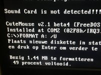
I just formatted a floppy disk without U87 in the socket and it's now completely working.
Another tense moment today because apparently I wasn't there yet, but it's all solved now, what a relief!
So here is the latest source for U87, where DMA is fully functional now.
These days I will be doing some more testing, if I find any problem I will post about it.
I just noticed that Disk Copy Fast is not working to write to a floppy, however I am able to write to a floppy and create a system disk without issues in DOS.
So maybe it's something in the code of disk copy fast.
Anyway, as long as I can write to a floppy normally, create a system disk and boot from floppy etc, it's fine by me.
It's -really- working now!
Turns out the problem with 8 bit DMA was caused by the CPU being inactive and not generating XBHE and XA0, which is then output by U87 instead on pins 15 and 16.
Not having these two signals there will not be any conversion happening during 8 bit DMA, which it needs. So U87 is actually activating itself by generating the conditions to do lower half of the databus conversions during 8 bit DMA when the CPU is inactive. So amazing how they used these pins for an output during 8 bit DMA to replace the absent CPU signals which at those times doesn't cause any contention, that's really some smart use of this PAL by IBM.
So what I commented on PA.EXE before about those OE equations was actually not correct, those equations are correct after all.
When I saw them I was initially thinking right away that that can't be right, but during DMA, of course, it is fine to generate output on these pins since the CPU is holding.
When compiling WinCupl threw an error because apparently AEN_1 & AEN_2 forms an "excessive number of terms for OE" or something along those lines.
Then I substituted DMA_AEN for this OE equation and it compiled without errors.
I just formatted a floppy disk without U87 in the socket and it's now completely working.
Another tense moment today because apparently I wasn't there yet, but it's all solved now, what a relief!
So here is the latest source for U87, where DMA is fully functional now.
Code:
Name     IBM-5170-U87 ;
PartNo   00 ;
Date     18-01-2023 ;
Revision 05 ;
Designer Rodney ;
Company  - ;
Assembly None ;
Location None ;
Device   G16V8A;

/* *************** INPUT PINS *********************/
PIN 15=XA0;
PIN 16=XBHE;
PIN 1=RAS;
PIN 2=MEMW;
PIN 3=IOR;
PIN 4=AIOW;
PIN 5=Q1;
PIN 6=IO_CS_16;
PIN 7=AEN_1;
PIN 8=AEN_2;
PIN 9=Q4;
PIN 11=FSYS_16;
PIN 13=RES_0WS;

/* *************** OUTPUT PINS *********************/
PIN 12=END_CYC;
PIN 14=DMA_AEN;
PIN 17=GATE_245;
PIN 18=DIR_245;
PIN 19=DATA_CONV;

!XBHE.oe    =  DMA_AEN;
 XA0.oe     = !AEN_2;
RES_0WS.oe = 'b'0;

XBHE      =  AEN_2 & !XA0;
XA0       = 'b'0;

DMA_AEN = AEN_1 & AEN_2;

!DATA_CONV =
    AEN_1 & AEN_2 & !FSYS_16 & Q1 & RAS & !XA0 & !XBHE
  # AEN_1 & AEN_2 & !IOR & IO_CS_16 & Q1 & !XA0 & !XBHE
  # AEN_1 & AEN_2 & AIOW & IO_CS_16 & Q1 & !XA0 & !XBHE;

!DIR_245 =
    !AEN_1 & MEMW & RAS
  # AEN_1 & AEN_2 & !MEMW & !XBHE
  # AEN_1 & AEN_2 & AIOW & !XBHE;

!END_CYC =
    FSYS_16 & Q1 & RAS
  # !IOR & !IO_CS_16 & Q1
  # AIOW & !IO_CS_16 & Q1
  # RAS & !RES_0WS
  # AIOW & !RES_0WS
  # Q4;

!GATE_245 =
    AEN_1 & AEN_2 & AIOW & IO_CS_16 & XA0 & !XBHE
  # AEN_1 & AEN_2 & !FSYS_16 & RAS & XA0 & !XBHE
  # AEN_1 & AEN_2 & !IOR & IO_CS_16 & XA0 & !XBHE
  # !AEN_1 & !AEN_2 & FSYS_16 & RAS
  # !AEN_1 & !AEN_2 & FSYS_16 & !IOR
  # !AEN_1 & FSYS_16 & RAS & XA0
  # !AEN_1 & FSYS_16 & !IOR & XA0;
These days I will be doing some more testing, if I find any problem I will post about it.
I just noticed that Disk Copy Fast is not working to write to a floppy, however I am able to write to a floppy and create a system disk without issues in DOS.
So maybe it's something in the code of disk copy fast.
Anyway, as long as I can write to a floppy normally, create a system disk and boot from floppy etc, it's fine by me.
Attachments
Last edited:
Hi Johann,
I just checked, my GAL is 25ns, which is what I am testing with.
Possibly 15ns will also be fine, however it's untested.
Hopefully you can get some good parts.
If they at least program and verify correctly that would be a good starting indication that they may be working parts.
Apparently GALs are sensitive, since two died during my tests.
I also read in some documentation about possibly having 100 write cycle limit, so this may have produced some wear during my work.
I think I must have programmed it at least 30 times.
About Disk Copy Fast, it turned out to work fine, I made a mistake in controlling it.
I have had too little sleep because of these GAL problems.")
It will be great to have some more testing done, so please let me know how it goes with his tests.
I just added a Trust 16 bit sound card and tested all the demo sounds and music in DOS which is also working fine with the replacement GAL, another good test of DMA.
I just checked, my GAL is 25ns, which is what I am testing with.
Possibly 15ns will also be fine, however it's untested.
Hopefully you can get some good parts.
If they at least program and verify correctly that would be a good starting indication that they may be working parts.
Apparently GALs are sensitive, since two died during my tests.
I also read in some documentation about possibly having 100 write cycle limit, so this may have produced some wear during my work.
I think I must have programmed it at least 30 times.
About Disk Copy Fast, it turned out to work fine, I made a mistake in controlling it.
I have had too little sleep because of these GAL problems.
It will be great to have some more testing done, so please let me know how it goes with his tests.
I just added a Trust 16 bit sound card and tested all the demo sounds and music in DOS which is also working fine with the replacement GAL, another good test of DMA.
Eudimorphodon
Veteran Member
Turns out the problem with 8 bit DMA was caused by the CPU being inactive and not generating XBHE and XA0, which is then output by U87 instead on pins 15 and 16.
Not having these two signals there will not be any conversion happening during 8 bit DMA, which it needs. So U87 is actually activating itself by generating the conditions to do lower half of the databus conversions during 8 bit DMA when the CPU is inactive. So amazing how they used these pins for an output during 8 bit DMA to replace the absent CPU signals which at those times doesn't cause any contention, that's really some smart use of this PAL by IBM.
Man, I wish I'd looked more carefully at the schematics earlier, because this is exactly the situation I was thinking of when I brought up how OE on a PAL can let a pin act as both an input and an output. Because of how the schematic was drawn I just assumed that everything on the left side was just an input and concentrated on just looking for possible other drivers or pull ups on just the pins coming out of the right half.
Here are my notes of reasoning about reduction of the product terms in !GATE_245
The square bracketed terms have been removed in the 5th revision U87 replacement GAL.
The equations for XA0 and XBHE have provisions for DMA controller 1, DMA controller 2 and ISA bus master cards.
Code:
REVISION 5:

!GATE_245 =

8 BIT DMA: (DMAC-1)
[   !AEN_1 & FSYS_16 & RAS & !XBHE ]             !!REMOVED XBHE = 0 UPPER BYTE CONVERSION ONLY SEE BELOW FOR BUS MASTERS
[   !AEN_1 & FSYS_16 & !IOR & !XBHE]             !!REMOVED XBHE = 0 UPPER BYTE CONVERSION ONLY SEE BELOW FOR BUS MASTERS
  # !AEN_1 & FSYS_16 & RAS & XA0            XA0 = 1                UPPER BYTE CONVERSION
  # !AEN_1 & FSYS_16 & !IOR & XA0            XA0 = 1                UPPER BYTE CONVERSION

ISA BUS MASTER DMA ON A CARD:
  # !AEN_1 & !AEN_2 & FSYS_16 & RAS            BUS MASTER MEMORY READS OR WRITES FROM 8 BIT MODE RAM TO 16 BIT RAM
  # !AEN_1 & !AEN_2 & FSYS_16 & !IOR            BUS MASTER 8 BIT IO READS TO 16 BIT RAM

CPU:
  # AEN_1 & AEN_2 & !FSYS_16 & RAS & XA0 & !XBHE    CPU ACCESS TO 8 BIT MEMORY ON UPPER BYTE OF DATABUS
[ # AEN_1 & AEN_2 & !FSYS_16 & !MEMW & XA0 & !XBHE]      !!REMOVED  BECAUSE !MEMW = 1 <=> RAS = 1

  # AEN_1 & AEN_2 & !IOR & IO_CS_16 & XA0 & !XBHE    16 BIT IO READS BY CPU TO UPPER BYTE OF DATABUS IN 8 BIT MODE
  # AEN_1 & AEN_2 & AIOW & IO_CS_16 & XA0 & !XBHE;    16 BIT IO WRITES BY CPU FROM UPPER BYTE OF DATABUS IN 8 BIT MODE
The square bracketed terms have been removed in the 5th revision U87 replacement GAL.
The equations for XA0 and XBHE have provisions for DMA controller 1, DMA controller 2 and ISA bus master cards.
Code:
 XBHE = AEN_2 & !XA0;
!XBHE.oe = AEN_1 & AEN_2;

 XA0 = 'b'0;
 XA0.oe = !AEN_2;

DMA 1:
XBHE = enabled, output by U87, inverse level of XA0
XA0 is not enabled as an output, provided by DMAC-1 during 8 bit DMA
with XBHE - XA0 = 1 - 0 and 0 - 1, there will always be conversions happening, up or down direction determined by DIR_245 output

DMA 2:
XBHE = 0
XA0 = 0
both generated by U87
which results in 16 bit mode for all operations by DMAC-2

DMA BUSMASTER:
XBHE = 0
XA0 = 0
both generated by U87
conversion will happen in case of 8 bit IO devicesMan, I wish I'd looked more carefully at the schematics earlier, because this is exactly the situation I was thinking of when I brought up how OE on a PAL can let a pin act as both an input and an output. Because of how the schematic was drawn I just assumed that everything on the left side was just an input and concentrated on just looking for possible other drivers or pull ups on just the pins coming out of the right half.
I appreciate your participation Eudimorphodon. The more people look at something, the better the chance of cracking it finally.
It was helpful to get your feedback about what's possible with PALs.
Before I cracked the final simplification this morning, I was also considering making a fuse map by hand because WinCupl simply was refusing to use my simplifications. Making your own fuse map is a lot of work and a lot more difficult, but it does allow total control and implementing your own ideas the way you want.
Also I saw some other methods on GitHub using some scripts to control Cupl compiler and some other fitters.
Besides getting U87 to work, I am kind of done with GAL chips, and in the future I will prefer to use CPLDs instead as discussed with lowen.
This problem of U87 was quite complicated. Especially since during certain input combinations XA0 and/or XBHE were acting as an output, thus throwing off the EPROM reads. The EPROM programmer was controlling XA0 and XBHE, while internally the GAL was providing other values to XA0 and XBHE. And there we go confusion starts to set in.
Anyway, I am happy I finally have a working GAL and some explanations for everything. And no decapping was needed! This is the only inportant result for me. I lost 3 weeks of work on this during the holidays building various adapters, testing software, etc. But it was well worth it in the end. There were times when I thought I will not see a GAL running in U87 socket. Not that I would give up, but I was just not seeing it yet at times.
Look at the design, the more I learn about it, the more I appreciate and respect all of it.
Seeing their work, I can get a better impression of the very creative IBM designers.
Any GAL16V8 should do besides the issue of speed which I wrote about, where I was not able to test a 15ns GAL yet.Can I use any GAL16V8 dip-20 part from ebay
I have tested with whatever I could find, all old parts. I reprogrammed a few Lattice GAL16V8A 25ns and one National Semiconductor GAL16V8A 15 ns. Though the National part died pretty soon so I was not able to test the operation if this was okay in the 5170.
If I find any other brand/speed GALs anywhere in my parts and PCB supply I will test them out.
I checked some old boards but mostly it's PALs which I can't erase.
If your programmer doesn't have the chip manufacturer and type, I suggest you select a Lattice GAL16V8A part if available. This selection allowed me to program the National IC as well at least.
Hi Johann,
That's very kind and helpful, all help is very welcome. I will PM you my address, thank you for this!
I have done extensive testing on the Lattice GAL16V8A replacement of U87, and everything is looking very good, I have found no issues with it. I have played various music files, including MOD files on the Soundblaster compatible Trust card which seems to work without any glitches. I will test everything I can find here and compare it with U87.
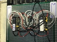
I am working on U130 right now, I just desoldered it from the 5170.
It is in poor corroded condition due to moisture exposure of the whole PCB, but it looks like I got a good read from the chip, lots of data showed up and a verification read checked out.
I am doing the EPROM mode minimizations according to the PA.EXE method, just as an initial indication of the structure of the chip.
I already saw that the unconnected output pins are used for intermediate functions.
I will first attempt a recreation to see if the minimized equations are valid.
Of course, as I mentioned in my previous posts about U130, I will be aware of checking where a latch was created by IBM.
This is necessary for the cpu / coprocessor interaction where a latched state is required, and not present anywhere in the 5170 so it must be in U130.
I will draw out a gate representation of some of the equations of U130 which should hopefully reveal where the latch was created.
A simple minimization of everything will probably not reveal any latches unless it's clearly present on the pins.
After U130 is finished and functional I will create a test version of my complete new memory subsystem. This needs a lot of connections and is also suitable to be done with programmable logic which will reduce the number of ICs a lot.
I am not sure yet if I will design an ISA card but I probably should because it's a lot of wires if I want to do it manually.
Maybe I will work on that card design this weekend so I can order it faster. The advantage of such a card is also that I can test all the RAM, BIOS ROM and option ROM together on one board, perhaps I will add almost the complete memory map in SRAM chips.
I mean, right now the CPU is slow, but it's entirely possible that later I will be testing a much faster and more capable CPU like a 486SLC or similar, and this may need more memory to test out things such as windows 95 for example.
I will do more research about the top of the 286 AT memory map, I read somewhere that perhaps part of this area should be avoided to put RAM memory there, and there may be some mirroring of the BIOS somewhere as well. It depends on the information I can find what I will do.
I could design a second ISA card to test the IDE interface, floppy drive and other stuff, and connect everything with the 5170 to have the whole design verified first. I also want to include a simple SCSI interface just for easy backups on an external harddisk.
The biggest step forward are the PALs and also the redesign of all the DMA logic where I have removed the refresh circuits and modified everything to work without them. Of course I will need to test this method first on the 5170, a lot of modifications are needed, I will solder in sockets for the ICs involved.
The most time will be needed to deliver the test PCBs from China so I will try to do this work sooner. And I will also order some CPLDs for experimenting with.
That's very kind and helpful, all help is very welcome. I will PM you my address, thank you for this!
I have done extensive testing on the Lattice GAL16V8A replacement of U87, and everything is looking very good, I have found no issues with it. I have played various music files, including MOD files on the Soundblaster compatible Trust card which seems to work without any glitches. I will test everything I can find here and compare it with U87.
I am working on U130 right now, I just desoldered it from the 5170.
It is in poor corroded condition due to moisture exposure of the whole PCB, but it looks like I got a good read from the chip, lots of data showed up and a verification read checked out.
I am doing the EPROM mode minimizations according to the PA.EXE method, just as an initial indication of the structure of the chip.
I already saw that the unconnected output pins are used for intermediate functions.
I will first attempt a recreation to see if the minimized equations are valid.
Of course, as I mentioned in my previous posts about U130, I will be aware of checking where a latch was created by IBM.
This is necessary for the cpu / coprocessor interaction where a latched state is required, and not present anywhere in the 5170 so it must be in U130.
I will draw out a gate representation of some of the equations of U130 which should hopefully reveal where the latch was created.
A simple minimization of everything will probably not reveal any latches unless it's clearly present on the pins.
After U130 is finished and functional I will create a test version of my complete new memory subsystem. This needs a lot of connections and is also suitable to be done with programmable logic which will reduce the number of ICs a lot.
I am not sure yet if I will design an ISA card but I probably should because it's a lot of wires if I want to do it manually.
Maybe I will work on that card design this weekend so I can order it faster. The advantage of such a card is also that I can test all the RAM, BIOS ROM and option ROM together on one board, perhaps I will add almost the complete memory map in SRAM chips.
I mean, right now the CPU is slow, but it's entirely possible that later I will be testing a much faster and more capable CPU like a 486SLC or similar, and this may need more memory to test out things such as windows 95 for example.
I will do more research about the top of the 286 AT memory map, I read somewhere that perhaps part of this area should be avoided to put RAM memory there, and there may be some mirroring of the BIOS somewhere as well. It depends on the information I can find what I will do.
I could design a second ISA card to test the IDE interface, floppy drive and other stuff, and connect everything with the 5170 to have the whole design verified first. I also want to include a simple SCSI interface just for easy backups on an external harddisk.
The biggest step forward are the PALs and also the redesign of all the DMA logic where I have removed the refresh circuits and modified everything to work without them. Of course I will need to test this method first on the 5170, a lot of modifications are needed, I will solder in sockets for the ICs involved.
The most time will be needed to deliver the test PCBs from China so I will try to do this work sooner. And I will also order some CPLDs for experimenting with.
Eudimorphodon
Veteran Member
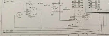
Of course, as I mentioned in my previous posts about U130, I will be aware of checking where a latch was created by IBM.
This is necessary for the cpu / coprocessor interaction where a latched state is required, and not present anywhere in the 5170 so it must be in U130.
I don't have the bandwidth at the moment to try to navigate this thread to find your draft of the U130 equations and I'm not sure what leads you to the conclusion that there needs to be a latch inside the PAL. I'm looking at this 80287 datasheet, page 5 and the description of what signals need to be latched on page 4, and my ignorant take on it is everything that needs to be latched should be directly covered by or could be synthesized from the address and signal latches U56, 60, 65, and 73 on 5170 schematic sheet 4?
... I mean, I guess there certainly *could* be a simple flip-flop/latch implemented in pins 13-16 since, they do appear to be NC on the schematic and all of them have feedback, so I won't rule it out.
It doesn't matter Eudimorphodon.
I also don't have the motivation to really dive into this PAL U130.
Since before I already sorted out what should be done for the coprocessor to function.
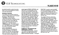
It's not too complicated and it's described by IBM in the 5170 technical manual, seen in the Copam501 and written about in VLSI documentation of chipset ICs.
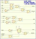
From all these sources I have drafted the schematic as seen in the KiCad screenshot, it can be found in the attachment.
Just for a try since it doesn't take much time, I have minimized U130 and programmed the results into a GAL.
During Landmark and Checkit tests using the GAL for U130 I can see the NPU performance so it seems to work at those tests, but I highly doubt that the equations are complete. It looks like some feedback got lost in the minimizations.
When I look at a gate representation I am seeing open ends.
And IBM did some weird stuff because they tied pin 11 to ground.
It seems they had some application but built in the option to disable certain logic by tying pin 11 to ground.
This generates 1 and 0 in the appropriate areas to disable the influence of pin 11.
Actually the NPU control is so simple that I will probably not be using these equations and spend days to write out equations and drawing gates, I will simply use the KiCad version in my attachment which reflects all the source information.
Those ICs you mentioned are bus transceivers and not involved in coprocessor latching of the ERROR condition.
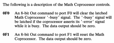
/ERROR:
an error status input from the coprocessor
this reflects the ES bit of the coprocessor status word and indicates that an
unmasked error condition exists
The coprocessor asserts /BUSY_287 when it is executing a task.
This is passed through to the CPU on input /BUSY_286
Normally /BUSY_286 will follow /BUSY_287,
however if /ERROR is asserted while /BUSY_287 is active,
the /BUSY_286 output will be latched low and remains low,
until it is cleared by an IO write cycle to 0F0 or 0F1.
(0F0 = clear latched ERROR, 0F1 = reset the 287)
/IOW and 0F1 asserts a /RESET_287.
I can't really test the ERROR condition of the coprocessor because I don't know how to cause such a condition.
I don't know if those performance tests also check this function or not.
However all the descriptions are so clear I feel it can't miss. From the description in the IBM manual alone the circuit with a latch can be created and the Copam circuit diagram confirms this.
I will just implement the logic I created in mid december last year, and use a GAL to generate the decoding and control a normal latch IC as in the KiCad. So the gates will be replaced by programmable logic. I believe this is also what Copam did from their schematic. If there is any problem I can reprogram the GAL or whatever is used to test further.
I just post all these things here together in case someone is also searching for it.
Here is the result of the PAL read and minimization, however I don't believe it is fully functional to latch the ERROR condition of the NPU, so no guarantees, and I rather say it will probably fail at a real ERROR condition of the coprocessor, that's what I expect.
Rather, these equations at least allow the NPU to be able to pass some Landmark and Checkit testing without any crashes.
Unlike U87, U130 is not so essential to have a functioning AT, only important for the NPU to be fully functional.
In fact, U130 can be left out completely, which will only result in the NPU not being visible for programs which try to use it.
I will do some testing with the prototype to determine if the NPU functions.
I will do some research later about what could create those ERROR conditions so this can be fully tested.
I also don't have the motivation to really dive into this PAL U130.
Since before I already sorted out what should be done for the coprocessor to function.
It's not too complicated and it's described by IBM in the 5170 technical manual, seen in the Copam501 and written about in VLSI documentation of chipset ICs.
From all these sources I have drafted the schematic as seen in the KiCad screenshot, it can be found in the attachment.
Just for a try since it doesn't take much time, I have minimized U130 and programmed the results into a GAL.
During Landmark and Checkit tests using the GAL for U130 I can see the NPU performance so it seems to work at those tests, but I highly doubt that the equations are complete. It looks like some feedback got lost in the minimizations.
When I look at a gate representation I am seeing open ends.
And IBM did some weird stuff because they tied pin 11 to ground.
It seems they had some application but built in the option to disable certain logic by tying pin 11 to ground.
This generates 1 and 0 in the appropriate areas to disable the influence of pin 11.
Actually the NPU control is so simple that I will probably not be using these equations and spend days to write out equations and drawing gates, I will simply use the KiCad version in my attachment which reflects all the source information.
Those ICs you mentioned are bus transceivers and not involved in coprocessor latching of the ERROR condition.
/ERROR:
an error status input from the coprocessor
this reflects the ES bit of the coprocessor status word and indicates that an
unmasked error condition exists
The coprocessor asserts /BUSY_287 when it is executing a task.
This is passed through to the CPU on input /BUSY_286
Normally /BUSY_286 will follow /BUSY_287,
however if /ERROR is asserted while /BUSY_287 is active,
the /BUSY_286 output will be latched low and remains low,
until it is cleared by an IO write cycle to 0F0 or 0F1.
(0F0 = clear latched ERROR, 0F1 = reset the 287)
/IOW and 0F1 asserts a /RESET_287.
I can't really test the ERROR condition of the coprocessor because I don't know how to cause such a condition.
I don't know if those performance tests also check this function or not.
However all the descriptions are so clear I feel it can't miss. From the description in the IBM manual alone the circuit with a latch can be created and the Copam circuit diagram confirms this.
I will just implement the logic I created in mid december last year, and use a GAL to generate the decoding and control a normal latch IC as in the KiCad. So the gates will be replaced by programmable logic. I believe this is also what Copam did from their schematic. If there is any problem I can reprogram the GAL or whatever is used to test further.
I just post all these things here together in case someone is also searching for it.
Here is the result of the PAL read and minimization, however I don't believe it is fully functional to latch the ERROR condition of the NPU, so no guarantees, and I rather say it will probably fail at a real ERROR condition of the coprocessor, that's what I expect.
Rather, these equations at least allow the NPU to be able to pass some Landmark and Checkit testing without any crashes.
Code:
Name     IBM-5170-U130 ;
PartNo   00 ;
Date     19-01-2023 ;
Revision 01 ;
Designer Rodney ;
Company  - ;
Assembly None ;
Location None ;
Device   G16V8A;

/* Dedicated input pins */

pin 1   = RESET;     /* Input */
pin 2   = ERROR;     /* Input */
pin 3   = 287_BUSY;  /* Input */
pin 4   = XA0;       /* Input */
pin 5   = XA3;       /* Input */
pin 6   = XIOW;      /* Input */
pin 7   = SM_IO;     /* Input */
pin 8   = 287_CS;    /* Input */
pin 9   = INTA;      /* Input */
pin 11  = 11_NUSED;  /* Input */

/* Programmable output pins */

pin 12  = NPCS;      /* Combinatorial output */
pin 13  = 13_NUSED;  /* Combinatorial output */
pin 14  = 14_NUSED;  /* Combinatorial output */
pin 15  = 15_NUSED;  /* Combinatorial output */
pin 16  = 16_NUSED;  /* Combinatorial output */
pin 17  = RESET_287; /* Combinatorial output */
pin 18  = IRQ13;     /* Combinatorial output */
pin 19  = 286_BUSY;  /* Combinatorial output */

/* Output equations */

!286_BUSY =
      !287_BUSY
    # 11_NUSED;

!IRQ13 =
      ERROR
    # 287_BUSY;

!RESET_287 =
      !RESET & !XA0
    # !RESET & XA3
    # !RESET & XIOW
    # !RESET & SM_IO
    # !RESET & 287_CS
    # !RESET & !INTA;

!16_NUSED =
      RESET
    # !XA3 & !XIOW & !SM_IO & !287_CS & INTA;

!15_NUSED =
      11_NUSED
    # !RESET & !ERROR & !287_BUSY & XA3
    # !RESET & !ERROR & !287_BUSY & XIOW
    # !RESET & !ERROR & !287_BUSY & SM_IO
    # !RESET & !ERROR & !287_BUSY & 287_CS
    # !RESET & !ERROR & !287_BUSY & !INTA;

!14_NUSED =
      ERROR
    # 287_BUSY
    # 11_NUSED
    # !RESET & XA3
    # !RESET & XIOW
    # !RESET & SM_IO
    # !RESET & 287_CS
    # !RESET & !INTA;

!13_NUSED =
      RESET & !11_NUSED
    # ERROR & !11_NUSED
    # 287_BUSY & !11_NUSED
    # !XA3 & !XIOW & !SM_IO & !287_CS & INTA & !11_NUSED;

!NPCS      =
    XA3 & !SM_IO & !287_CS & INTA;
Unlike U87, U130 is not so essential to have a functioning AT, only important for the NPU to be fully functional.
In fact, U130 can be left out completely, which will only result in the NPU not being visible for programs which try to use it.
I will do some testing with the prototype to determine if the NPU functions.
I will do some research later about what could create those ERROR conditions so this can be fully tested.
Attachments
Last edited:
Eudimorphodon
Veteran Member
From all these sources I have drafted the schematic as seen in the KiCad screenshot, it can be found in the attachment.
I posted a link earlier to how to implement a latch on a GAL; if I’m understanding your schematic correctly if there is a latching action there I would wager that you’re going to see that one of those NC pins on the original PAL is “paired” to IRQ13 for the latching action and its feedback state goes to the BUSY_286 equation. If you re-analyze the state results for the NC pins with this in mind you might be able to suss it out…
But, yeah, if the goal here isn’t to clone the PAL but to clone the machine then, sure, there’s no point.