• Please review our updated Terms and Rules here

Project to create an ATX 80286 mainboard based on the IBM 5170

And here are the equations I get for this IDE/floppy controller:

Code:
!FDC_LDORn = SA1 & SA4 & SA5 & SA6 & SA7 & SA8 & SA9 & !AEN & !SA0 & !SA2 & !SA3
!FDC_LDORn.OE = 0
!FDC_LDCRn = SA0 & SA1 & SA2 & SA4 & SA5 & SA6 & SA7 & SA8 & SA9 & !AEN & !SA3
!FDC_LDCRn.OE = 0
!IDE_CS1n = SA1 & SA2 & SA4 & SA5 & SA6 & SA7 & SA8 & SA9 & !AEN & !SA3
!IDE_CS1n.OE = 0
!FDC_CSn = SA2 & SA4 & SA5 & SA6 & SA7 & SA8 & SA9 & !AEN & !SA1 & !SA3
!FDC_CSn.OE = 0
!LSPIN9 = FDC_DCn
!LSPIN9.OE = 0
!IDE_CS0n = SA4 & SA5 & SA6 & SA7 & SA8 & !AEN & !SA3 & !SA9
!IDE_CS0n.OE = 0

I didn't check in detail but they seem to be identical to the ones you got from PA.EXE. Rodney.
 
It turns out that the script code was only looking at the PAL input coming from the address lines of the "EPROM dumper". The PAL input coming from the PAL itself (again, our beloved "cascaded PAL pins" topic...) is ignored.

At the end it turned out that when creating the equations, it is necessary to check if A10-A17 match D0-D7. If this does NOT match, we are currently checking an input which the PAL never sees, because it is internally setting an input pin, overriding what is set by the "EPROM dumper". To boolean algebra, this translates to "don't care" - input which is never seen does not need to be handled in any way, it is irrelevant if low or high is generated. With this information, sympy has the opportunity to simplify "sufficiently".
Johann, absolutely brilliant deductions, my compliments for your work!

This kind of conclusion is that type of critical reasoning where once you realize it or read it, it totally makes sense, but the process of arriving at the specific conclusion, that is the really tough process to be able to get there. Evidently, this new script of yours is advancing PAL analysis to a whole new level!

When I started to realize that the creation of new terms was happening from the EPROM reads due to the "cascading" internally in the PAL, I could see the problems arising from PA.EXE outputs, and that these could not be taken literal in all cases. Now you have improved upon this so much by automating the process! This really shows where creative programming can solve all sorts of complex problems.

I only wish we can have more "test subjects" to see how these turn out. If I find any more important PALs to analyse, I will add them to this thread. Maybe I have some arcade PCBs which contain some.

Really interesting and remarkable that you have found that certain logic states consist of invalid information, as you have clearly described the reason for it happening in your example. The PAL is basically not listening to the input states in that result reading, so that reading is not correctly reflecting what is happening.

Thanks for your hard work on this Johann!
 
I didn't check in detail but they seem to be identical to the ones you got from PA.EXE. Rodney.
Thanks Johann for checking this, it's good to have the extra check from your new script.
I have verified the equations with my information, it's completely identical with yours, and there is nothing complex going on there in this PAL at all.

Analyzing this really useful floppy/IDE card which came in a 286 PC a neighbor gave to me long ago has shown how they solved this problem of overlap in IO ports between the floppy and IDE port.

The floppy /DC signal even feeds into the transceiver of the IDE port which I won't be doing, I prefer to keep devices separate and not using eachother's ICs. I will feed /DC straight into SD7 using a LS125 gate after inverting it, as I did before on my XT.

Either way, there should not be any conflict as they have even wired it onto the IDE side of the transceiver on this card which tells us that the IDE will not be active while reading this value, so the FDC must be reading port 3F7 to get the /DC information, and the IDE controller in PC IDE harddisks should not be responding to port 3F7 reads even while there is a /CS1 decoded active on it, so it must be some kind of "ignore" condition for the harddisk controller.

I have worked more on the designs and now finished sorting out which logic goes into which of the three CPLDs, and I am checking the signal flow to be accurate across them and in correspondence with all the mainboard functions.

There is a small matter of when I add a bidirectional or output pin in a CPLD which uses a tri state enable function to connect with a circuit output in the quartus schematic, whether this will be directly translated to a tri-state OE function on the output pin itself by using the "tri" element in quartus in those areas.

I can't be 100% sure whether the CPLD when programmed will actually translate this to perform this function on the outside since I have never tested this before, so for safety sake, I will be adding a few separation resistors on those pins so in case there is any contention happening because of programming problems, at least it won't damage these CPLD outputs. If anyone can comment here in time, I could remove the resistors from the design when I know it to function properly for certain.

There is really little to no documentation of functioning of the logic elements in the CPLD which are provided by quartus itself as elements in the schematic design program. Though I did get some compile errors when I used a certain other type of tri-state element where quartus reported that this element was not compatible with the CPLD type we are using. So that gives me hope that things will function as intended on the output or bidirectional pin since quartus does check various things which is helpful. When I don't see any problems and the system is functioning I can try removing the separator resistors and bridging these. It only concerns 3 pins. I will use low value resistors for testing. The problem with quartus and designing CPLDs is that mostly they focus on VHDL and more complex applications, where I only need some basic logic operations for the AT system in this application just for the sake of reducing the total PCB size. Maybe later I can get the VHDL logic equivalents of the design and compare it with the schematic to see how one translates into the other, which is interesting, but also would consume a lot of time to study it, and I do want to progress in this project to the end result sooner.
 
For those following my project, I am currently looking at a first PCB layout just to get a sense of what the whole system looks like on a PCB, which to me is a big milestone looking back at the difficult development for this project. The AT was definitely more complex and difficult to achieve a full circuit which should be functional, but now we have passed this point, the final result is going to be taking form in the layout.

Doing this test layout can provide a good first impression whether the system in the current form can actually fit on the PCB area.
Also it has the advantage that I can see the pin layouts of the CPLDs now to further adapt them to suit the layout and PCB traces.
The CPLDs are really flexible which inputs and outputs you want on which side, and in which order of pin numbers. There are only a few pins which only can become inputs because they are global inputs. As I understand it, these can be used just like any normal other input if the application suits this.

In the past I have had ideas which were too big to fit on a whole mainboard, which can only become apparent when actually putting the components on the PCB, so it may become necessary to move certain things off the PCB in case the whole system can't fit on the PCB space. I have thought about shifting certain areas to additional PCBs but my preference is to create a single board which contains most of the parts.

I will attempt to optimize the layout and fit as many circuits on the mainboard as possible. Hopefully I can keep the printer port because I like to be able to use interlnk/intersvr to transfer files in DOS.

As I mentioned before, I am going to put all the SRAM ICs on a single plug in PCB to save the typical PCB space which early mainboards allocated to RAM. This PCB can be any size from very small for example 4MB until 15MB of SRAM which is fully decoded in the memory CPLD. The option ROM is also present on the mainboard which enables booting from the XT-IDE AT IDE BIOS without needing additional cards. Total of 32kb option ROM space will be available.

I will also feature a Pi Pico for the serial to USB mouse function as mentioned before, so this will also become a vertical small PCB plugged into the mainboard since the Pico is also a considerable area which I want to save space on. The USB type A connector for a serial mouse will be featured on the IO shield area.

The design is not fixed persé at this time, and I will be doing more verifications on the circuits. If I find something which needs to be changed I will modify or redo the layout, however many of the circuits are now inside the CPLDs so these can be reprogrammed later at any time if needed so that's a big advantage. I expect that the circuit design is not going to change very much.

The memory CPLD has already found a permanent place in my current layout, the other two CPLDs are just loosely placed so they may be moved if needed.

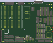
Just to get a picture of what the PCB is starting to look like, I have included a screenshot from the KiCad 3D viewer.
I am working my way through the PCB starting in the bottom right with the memory subsystem and the CPU.

It's my preference to do a two layer PCB if possible which will cost a lot less to manufacture of course.
 

Attachments

  • ATX 80286 Mainboard test layout.png
    ATX 80286 Mainboard test layout.png
    68.2 KB · Views: 15
After some test routing of traces, I checked on the website of JLCPCB and apparently ordering a 4 layer design still falls within a very reasonable price range, so I will continue the design in 4 layers.

This will at least make a closer spacing possible which will benefit the project a lot, I think I will be able to include all the intended components on the PCB, optimizing the PCB space usage.
 
Last edited:
I just want to update everyone following this project on my current development and design status.
Not that anyone could get the impression that it's not progressing, I can report, on the contrary of course.

I have worked really hard on the project doing several test layouts to determine a type of layout and placement configuration which feels right.
This aspect needs some careful attention, and work.

I have done a few layouts where I tried to keep the memory subsystem out of the way of the core system traces in order to be able to connect everything.
However the memory surface area needed due to the trace volume and components is still considerable, no matter which placements I use.

So one of the things I have decided to do yesterday is to remove the whole memory subsystem away from the mainboard and onto a ISA board.
Instead of using a custom RAM PCB with only RAM chips, which will be needing a separate PCB anyway, I am planning to move all of the memory onto a ISA card design.

Using one ISA slot of the 7 available slot positions for the memory subsystem is not a problem at all since this integrated design needs almost no additional cards except a VGA and soundcard. Using an ISA card also is more tidy when building a system with this mainboard.
It's a little involved and I need to look into how I will do this because the memory decoder CPLD is also decoding the coprocessor control which is connected to the mainboard.

Of course, nothing is confirmed yet but this is the path I am going to focus on now.
I hope this can then sufficiently enable me to do a complete layout which at the same time also feels good and right.

And afterwards I still need to do the extensive functional verification of the whole design in order to attempt to eliminate any possible errors.
Assembling this type of mainboard is also going to be a lot of work so I need to make sure of as many things as possible before hand, and then choosing a certain point where I say it's enough, and then let's produce the first PCBs.

I hope I can achieve a full design soon and order the PCBs, I am working hard on reaching this result!
Of course, I will eventually share everything from this project publicly.

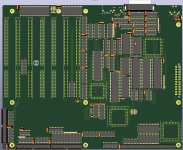
In attachment I have included a screenshot where the memory subsystem is still present on the PCB, so I will continue to the next test layout, hopefully it will become a keeper.
 

Attachments

  • PCB_screenshot_002.png
    PCB_screenshot_002.png
    119.8 KB · Views: 12
I'm wondering about timings. If it's targeting 6 or 8MHz, that might work okay. But if you wanted to use, say, a 16MHz 286, that would be feasible with the common 55ns SRAMs, but you don't want to run the rest of the ISA bus at 16MHz, and running at 8MHz would force wait states for memory.

If you wanted to put the RAM card in the place of an ISA slot, cool, but I'd wonder if it should be electrically different.
 
Hi Hak Foo, thanks for your message, it's nice to hear from you.

In my design, it is completely detached between the different clock speeds.
What I mean is, by reprogramming the system controller CPLD, the clock speeds on the ISA bus and the CPU are completely independently configurable from the internal system clocks such as the DMA controller clock, timer clock, keyboard controller clock etc.

Where the clocks are used for certain fixed or limited controller types such as the 8237 chips, timer and the keyboard controller, these are all generated in a fixed manner, independent of the CPU and ISA bus speeds. There I am using the optimal values in the CPLD design where for example we are going to attempt to clock the 8237s at 4.77 Mhz initially which seems optimal at the moment. Maybe they can go up to 5Mhz, I am not sure since I never tried that.

The ISA SYS_CLK signal can be varied because it's an output of the system controller CPLD, which we can reprogram if necessary.
Same goes for the CPU CLK of the 286.
I will publish everything as open source on my GitHub, it should be possible for advanced users to reprogram any CPLD to adjust these kind of things as they wish, of course anything a builder does is completely at their own risk what the consequences will be. So the system should be configurable and there is room for experimentation, which is of course at the user's own discretion and responsibility.

Also generally I want to comment here so everyone understands this concept. The ISA bus should not be seen as a "clocked" system, because basically it isn't. It is better to keep in mind that the ISA bus along with the entire AT system has certain timing restraints due to limits in certain critical circuit areas. I expect that using CPLDs, which are much faster logic, should have a positive influence on this aspect.

You commented about wait states on the ISA bus, actually the memory subsystem itself is not going to do this. There is no "intelligent" memory controller on the ISA RAM card which could decide to generate wait states. Only normal memory decoding is happening, and the type of RAM will be implemented as normal XMS memory on the ISA card. So you could say there is no limit posed in anything else than the pure memory speeds. Either the memory can keep up with the CPU, or it can't. This can only be found by doing some experimentation on the CPU clock speeds. Hopefully we can reach the 16Mhz you mentioned, which would be great of course.

The clock pulse SYS_CLK on the ISA bus will be used by certain ISA cards which are designed this way. However that is the choice of the designer, he also could have chosen to generate their own clock signals on the card which is not too difficult either.

The OSC signal is simply always a fixed clock of 14.318 Mhz which is a standard clock speed in the AT ISA standard.

On the other hand we have the concept of how fast the ISA bus access can function. This can only be determined by testing. If a certain card is clocked from the SYS_CLK, and the SYS_CLK is too fast causing that card to malfunction, that will cause certain stability issues when the card interacts with system memory and the CPU.

For example if a certain ISA card is a bus master, it may attempt to access the system memory in a higher speed than this memory can follow in a stable manner, which you also mentioned in your post about the RAM speeds having a certain specification limit. If that card is accessing a certain bus and expecting a certain relative propagation delay dependent response from the bus which is shorter than those transceiver specs, this also will cause issues, etc.

When a user wants to experiment, he should first study the cards he is going to use for example the VGA card, how is it clocked? By its own oscillator or from the SYS_CLK.
By studying how the card works, it can at least be possible to predict what will happen with a certain card by raising certain clock speeds.

Also, for speeding up the CPU, it's not necessary persé to also raise the SYS_CLK speed on the ISA bus.

Internally in the CPLD there are certain clock dependent circuits used to sync the CPU cycle transition timings and to time the byte conversions between 8 and 16 bit, however this is all also done in the system controller CPLD so internally these clocks will be varied along with a raised CPU clock speed, where it could at the same time be possible to output a typical fixed and lower 8Mhz SYS_CLK to the ISA bus since this is a normal output of the CPLD which is only routed to the ISA bus and nothing else on the mainboard depends on it, well, except the SCSI controller chip, which will be fine to keep running at 8 Mhz for example since it's not involved in any CPU synchronization or byte conversion timings anyway.

There is a separate 16Mhz clock generator provided on my mainboard which is connected with the system controller CPLD. This clock input will separately clock certain things which cannot and should not follow a raised CPU speed, which I am already doing in my CPLD design now. Also, for example for the DMA controllers which are very limited in their clock tolerance and quite easy to become unstable at faster clock speeds have their own clock derived from OSC. This really should not be increased beyond 5Mhz unless the user has an actual higher clock speed specification 8237 and knows what they are doing of course. Everything is at their own risk of components getting destroyed by overclocking of course.

So the CPU clock can be increased within reasonable confines of what the memory and bus transceivers can handle. Maybe 10, 12, 16M or higher. At the same time the SYS_CLK can be separated by changing the CPLD design slightly, and kept on the original constant 8Mhz while the CPU speed is raised. Or even maybe it can be possible to clock the ISA SYS_CLK to 10Mhz if anything is clocked by it such as a VGA card, to test overclocking the VGA card itself. This is perhaps a little risky to overheat and destroy a VGA card. The transceivers should be fast in their propagations since these are faster TTL types and these type of ICs are already manufactured faster by design, and a faster CPLD will also generate the transceiver controls much faster than normal TTL based circuits. I think the real limit will be posed by the SRAMs themselves. I have a number of SMD 4Mbit SRAMs which I removed from old equipment, I have not checked the specs of these chips at all yet. Also it should be possible to create a memory ISA card using other methods like a FPGA SDRAM or DDR controller which interfaces with the AT bus to provide the memory space. That's also a nice idea for the future as a project.

The user should observe the entire system when trying to create a faster system. For example if they want to increase the clock speed on a VGA controller which is clocked from the SYS_CLK, they can have a try to raise this clock speed separately and just see what will happen. Of course if this experiment breaks the VGA card, that is always their own responsibility when doing anything with my designs. But that is always the known risk when doing overclocking of any kind of course.

Another factor in speeding up the system whether it's possible at all is also the response time of the IDE harddisk. Since this contains the controller inside the drive, and I just checked, there is no wait state signal connected to the IDE bus, at least I don't remember ever seeing one so this is also dependent on the software to control a harddisk in the XT-IDE BIOS whether this contains routines which wait for the drive to actually respond before continuing. I did not have much experience in this area yet, but I will test out many things later. If a IDE drive is capable and able to generate wait states we could try to connect that to the ISA bus to support it. The floppy drive should not pose any problems because it's controlled by the 8237 on its own clock generator.

Alternatively it should become possible to exchange the whole CPU to an even faster type by doing emulation and including the RAM inside the emulation device. Then it could be possible to simply remove the memory subsystem ISA card from the mainboard and use the memory on the emulation device which can be much more modern and faster. Provided that the BIOS and option ROM code for booting a XT-IDE AT BIOS supported harddisk are included in the emulation device.

I may design a new mainboard later based on a faster 16 bit CPU such as the 486SLC or even possibly others.
Another future idea is to try to design a VLB system, I will spend time on studying this standard in the future.
Or even PCI though that will surely be even more difficult.
And I want to study 32 bit PC technology, how are they doing byte conversions etc, which I am more interested in now after working on this design.
Those are all things I plan to do in the future, step by step.
What I love the most is to get the maximum performance out of a limited technology, which is much more challenging than simply using a pentium class PC or even a P4 etc.
This concept started with the 8-bit XT, just to stretch the usage of this PC as far as possible.
Which I also will revisit in the future using CPLDs.

I want to try out a lot of software on this 286 project after it is functional, including new compilations of DOOM and I want to see how Wolf3D performs on it.

So for hopefully being able to play these performance dependent games even better I will also be looking at how I can speed up things later and if I do, I will share the findings here as well later on.

For the moment I must first get the whole system designed and functional which is still a lot of work ahead for me, and then it will be time to seriously play around on it, which of course is the best part of all that work.

I am starting to miss DOS gaming a lot because of always working on this project, so I will want to catch up on this as well soon.

Kind regards,

Rodney
 
Last edited:
I was probably oversimplifying things. I figured if the memory is on the same ISA bus as other devices, any memory access is going to toggle the address lines on that bus, and doing that at 16MHz might annoy ISA devices.

If it's on a separate bus, I could imagine only exposing accesses to the ISA bus if they're targeting parts of the address space where RAM isn't.

An interesting idea might be to provide a register that lets you change if memory reads in a specific range are mapped to the ROM or the RAM, so a shadowing routine could be enabled.
 
I was probably oversimplifying things. I figured if the memory is on the same ISA bus as other devices, any memory access is going to toggle the address lines on that bus, and doing that at 16MHz might annoy ISA devices.

AT bus machines that run (much) faster than 8mhz typically are designed so the effective system clock is controlled by a decode that senses if a memory or I/O read-write request is *not* targeted at a motherboard resource capable of handling the full CPU clock; if that’s the case the effective system speed is divided so there will be a reasonable chance that an ISA bus device designed for the original AT will work. (The earliest “Turbo AT” clones didn’t include this, and therefore would often have serious expansion card compatibility issues.)

Implementing this properly is a fair bit of work. Here’s a databook for the well regarded NEAT AT chipset; the description of the 82C211 clock generation and bus control component discusses how it handles transitioning between clocks on the zero crossings to prevent “runt” clock impulses. If you want to build a 286 motherboard that runs much faster than 8-10mhz or so that doesn’t have severe issues with ISA card compatibility you’ll need to implement a system like this.

To be clear, you certainly could implement this and still have all your RAM on a card that “looks like” a normal ISA card and plugs into the regular bus slot; if your speed-switching logic slows down appropriately when *not* accessing the memory region corresponding with the high-speed memory the other cards should be okay, the “too fast” transitions flying by on the bus wires *probably* shouldn’t upset them when they’re not selected… Although a possible edge case could exist if your *fast mode* is so fast that you‘re starting read/write cycles to the fast memory before the address decoding hardware on the slow ISA cards have made a definitive decision about whether they’re being addressed. If you were pushing up beyond 16-20mhz this actually could be a problem acute enough to argue for having the fast RAM on a privately buffered bus.
 
Hi Hak Foo,

Yes, it's interesting to use shadow ram to replace this in the memory space of the BIOS.
This feature is also done on my Z80 CP/M mainboard, and would need a combination of switching the memory decoder and doing a copy of the BIOS contents to that area first.
So the cache RAM should initially be presented in another location in memory space and then remapped by switching the memory decoder.
This should work, but would need some BIOS programming to be done to initialize it from the BIOS. Maybe a feature for later on after the system is working.

Hi Eudimorphodon,

Thanks for your information, you are giving me some ideas to think about which is great.

After verifying this project to be functional I will consider what the next steps will be.
I want to explore first what this design can reach as-is in terms of clock speed limits.
When there are some problems happening at higher clock speeds we can indeed think more about how to possibly solve those.
It will be interesting to observe what happens when speeding up the CPU.

Thanks for the link to the chipset documentation, I will download and read it, certainly very interesting. I have a Neat 286 PC here which runs at 16Mhz which is a very stable system which works well. Maybe this datasheet can inspire some new ideas. I will also read the VLSI documentation I have as well to see if I can find anything about this subject there.

If we desire even more speed, I think it may be also be worth considering to use an alternative CPU for example by some form of CPU emulation which includes its own RAM of a modern type. Emulating the CPU can exceed what typical 286 chips can do clock-wise. Since the CPU is emulated anyway, this poses less problems because the RAM is on the CPU's bus anyway and capable of running at the same speeds as the CPU emulator itself.

I think I should study the newer generation CPU types as well which are still running a 16 bit databus. This also opens up more software to be able to run on the system such as windows 95 for example. That is my original "next step" idea and I will look into this as well after finishing this 286 project. It's probably not too hard to redesign the mainboard and putting in a 486 SLC or something like that instead of the 286, it's worth a try, but I will need to study the target CPU carefully first to see if and how to do this. At least the CPU should support data byte conversion and provide compatible bus control to be able to be used as a replacement.

What I am doing in the current project, to physically move the RAMs, decoder and transceivers onto a custom ISA card of my own design is functionally exactly the same compared to originally having the RAM on the mainboard itself, there is no functional difference, bus connection/control difference or speed compromise involved there. I am obsering to keep compatibility with the 5170 design as well.

The current system will not be holding the CPU for doing DRAM refresh cycles which will provide a small performance advantage as well where the CPU doesn't need to wait for this.

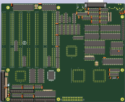
I have done some work on the new component placement and will be doing another test layout soon after finishing the component placement work, you can see my current design in the screenshot. I think this configuration has a chance of making it into the final design of the first prototype.

Thanks for your interest and ideas Hak Foo and Eudimorphodon!
 

Attachments

  • PCB_screenshot_003.png
    PCB_screenshot_003.png
    107.2 KB · Views: 4
If we desire even more speed, I think it may be also be worth considering to use an alternative CPU for example by some form of CPU emulation which includes its own RAM of a modern type. Emulating the CPU can exceed what typical 286 chips can do clock-wise. Since the CPU is emulated anyway, this poses less problems because the RAM is on the CPU's bus anyway and capable of running at the same speeds as the CPU emulator itself.

Of course, this raises the point that, well, DOSbox, MAME, and other perfectly good emulators already exist, but... whatever.

Once you start raising the ante with CPU speed it seems like the place you're going to naturally arrive at is a machine like the Tinyllama2, which repurposes a 500mhz-ish 486-like x86 SOC into a DOS-compatible PC. Which is cool, I guess? The one thing I suppose you don't get is an ISA bus... although technically according to the datasheet the Vortex86EX *does* support ISA... with some significant limitations. (Limited to a single DMA and interrupt, which would kibosh most sound cards.)

I think I should study the newer generation CPU types as well which are still running a 16 bit databus. This also opens up more software to be able to run on the system such as windows 95 for example. That is my original "next step" idea and I will look into this as well after finishing this 286 project. It's probably not too hard to redesign the mainboard and putting in a 486 SLC or something like that instead of the 286, it's worth a try, but I will need to study the target CPU carefully first to see if and how to do this. At least the CPU should support data byte conversion and provide compatible bus control to be able to be used as a replacement.

The 386sx (and by extension, those 486SLC-type CPUs) are almost entirely 286 compatible from an electrical standpoint; my vague recollection is there's like one or two bus control signals that need massaging to adapt a 286 motherboard to be 386sx compatible, IE, you can't do it with a *completely* passive adapter, but it's close. (I want to say that the "extra" signal on the 386SX has something to do with instruction pipelining, but I might be very wrong about that.) Strictly speaking the full-blown 386 (and I think even the 486) *could* be run on a 16 bit bus by just holding the bus sizing signals appropriately, but obviously there wouldn't be a lot of point to doing that.
 
Of course, this raises the point that, well, DOSbox, MAME, and other perfectly good emulators already exist, but... whatever.
There are always alternatives of course. Anyway playing those old games is always great fun, even on other platforms.

Well as for me and for my vision for the future, I'm going to build this machine which contains important parts of IBM's Don Estridges legendary secret sauce designs of 8 bit compatibility and I am trying to experience a historical feeling by following the footsteps of the IBM designers. I am doing my own version of approaching them. I will follow the natural process where this project leads me.

I would only use emulation in my projects where it can recreate the function of a single component of the system in the same manner but then faster or replacing technology which is also dying out due to recycled chip shortage etc, such as a CPU or VGA card, perhaps a PicoGUS and similar, and the 8237 etc should be replacable as VLSI and Neat have done before. While preferably not leading to a totally different system which is not compatible anymore, but rather to a faster version of the same functional technology. Like for example a replacement CPU in whatever technology where you can actually 1:1 plug it into a 5170 and it would actually work with that, this to me for example would be a successful replacement.

The Tinyllama project looks cool though, I just saw it, thanks for the link. I mean, to at least run DOS? that is interesting and a nice other kind of project. I love the Crystal sound chip and should remember looking into this in the future to try this chip out!

As I have mentioned my intention for the future, I will be looking at the 486SLC some time in the future. I should have one of these chips somewhere which I soldered onto a QDI 386 mainboard just for fun. I can remove it and repurpose it for interfacing it with this 16 bit AT system. And another idea is to study the technology of vesa local bus and PCI. If I see some way to implement a 32 bit system, I may go for that. It's a valuable learning experience for sure.

Thanks for your mentions of what you remember about the 386 and 486 Eudimorphodon, those are very useful points so thanks for that. I will keep your comments in mind when starting to do research for that future project. I will post a new thread about this when the time comes. By the way, using a 32bit 486 running in a kind of 16 bit mode is not something I would find useless persé, I would be willing to build this anyway. I mean it's another way to at least have a 486 functioning. Maybe this has certain other advantages over the 486SLC. Performance is not the reason for me to do these projects, it is especially for the learning experience, historical aspects and just to see what the limits of each system are in terms of what it can run. When designing a new system, it is great to make it exactly the way I envision it should become, this is another very attractive aspect for me.

Back to work for me, I will post some info about the progress for the mainboard and ISA RAM card designs. I will keep the EPROMs on the mainboard simply because I like it more that way and it looks cooler. Let's see if this latest placement is routable, if it can be done in a reasonable manner then I will see it through to manufacturing and the next step will be to test the system.

Kind regards,

Rodney
 
Thanks again everyone for all of your comments and ideas, I appreciate it very much!
I will have much more reading to do on the datasheets and other ideas from Eudimorphodon, I will definitely do this because I see the value in those points.
Everything I can find and read now will surely benefit this and future projects in some form.

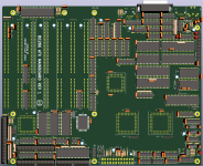
I finished the placement of all the components, if it's possible to fully route this PCB without needing to move anything, it's probably going to look close to this for the first revision, I included another picture of the 3D view. Maybe some people don't like the orientations of components, but this is just my style and habit. I also placed certain components underneath big ICs which will require to socket at least those ICs. There is simply too much advantage in the layout for me not to do this.

There is only one SMD component, the RTL8019AS LAN chip. Though if anyone who wants to build this mainboard doesn't want to solder this one, they can leave it and the serial EEPROM out.

The Raspberry Pi Pico will need to be soldered onto some sort of PCB to mount it vertically on the connector. This is also done to save valuable PCB space which this project really needs in order to be able to complete it. Wiring up the Pico is really straight forward and doesn't need too many connections, just a few serial lines, LED outputs, jumpers, power and the USB pins. It's on a 40 pin connector also for stability. As I commented before, this serial to USB mouse adapter by Adam (Limeprogramming) is really something I strongly recommend to try out, the mouse feels just as comfortable and responsive as on this modern PC I am writing with now. Any new project of mine which doesn't have PS/2 mouse input will definite;y feature this mouse adapter. Maybe I will make a small PCB later on with a RP2040 chip and a few support components for an even smaller footprint version of this mouse adapter where the USB is also taken out to normal pins that can plug into a mainboard, that would be really elegant to do it that way and it's something that I am planning for later.

I still need to add a few capacitors on the ISA bus to clean up certain lines such as RESET_DRV and others which are sensitive to reflections and crosstalk noise.
Especially positive active signals are more vulnerable to this, though I can only know what will happen when I can actually probe the pins later on, on the prototype itself.

After finishing the mainboard I still need to do the ISA RAM card.

We are not there yet, but I do feel it's a kind of milestone to arrive at this point where we are at right now.
I will do a lot of careful verification work as a last step in order to attempt to eliminate any possible issues later on.

Hopefully all the modifications to the CPLD version are going to work out without any major problems.
This will be my first CPLD supported project so I am looking forward to getting more experience with this and using this technology more in the future, and possibly also working with some FPGAs as well.

Kind regards,

Rodney
 

Attachments

  • PCB_screenshot_004.png
    PCB_screenshot_004.png
    143.3 KB · Views: 8
Hi Rodney,

I read through the last couple of posts, but I'm still a little puzzled.

Looking at the 80286 pinout, it seems to me it has a very "classic" design: address bus, data bus, a few control lines and exactly one clock (named CLK). Connecting SRAM to it somehow seems obvious with "masking out" the range above 640 kB being the only major challenge?!

Looking at the ISA bus, I also see only one clock (again, named CLK). I guess this originally was the CPU clock (for 6 to 8 MHz 80286), but with increasing CPU clock speeds this was the limited (to 8 MHz?) to stay compatible with ISA cards? So it should run completely asynchronous to the CPU clock and somehow, data must be buffered between CPU and ISA bus.

Now, how would you connect the SRAM via ISA bus and still have maximum performance, when the ISA bus is limited to 8 MHz?

Wouldn't it be easier to design some RAM daughter board connected via PIN header or similar? Then it could also be closer to the CPU...

Cheers,
Johann
 
Ok, after reading Eudimorphodon‘s post again, I understood that the clock on the ISA bus could be switched between full CPU speed and, e.g., 8 MHz. Sounds scary to me, but I‘m more or less a novice for such stuff. I still would think that a proprietary RAM expansion connector would simplify the design?
 
Hi Johann,

It's nice to hear from you. After doing many Z80 systems before, I can say I have a perspective on where the PC design is different from a more simple design such as a Z80. In the beginning I was kind of annoyed by this but further along I am starting to appreciate the brilliance of the PC design and it's particular advantages. The PC concept simply involves many things and this is the challenge to study and explore all of them. Since you are a programmer, perhaps you will enjoy to do some PC programming later on. With your amazing skill, you could possibly create some cool new stuff, there are still things not made yet which could be programmed. I don't remember specific examples right now but when I remember some I will mention it in this thread. But I know you are really busy and not too much time available at the moment. So I appreciate you taking the time to check in and read up on our project's progress.

I will try to share a few things, but really the best thing is to just study the 5170 design and XT design in much detail where you need to look at how everything functions many times to gain the complete instinctive insight. The disadvantage and challenge for any person is, this takes a lot of time and effort. But of course in our project's case, there was no getting around doing this work. The point which any engineer faces is to need to study the whole system with a specific purpose in mind of what you are trying to do with the whole thing and how you are going to interface a specific type of addition to it. In this case let me concentrate mostly on memory control since that is our recent point of discussion. After studying the system so extensively for many hours which was absolutely necessary for doing this project, I am glad to share some insights, after all that is the purpose of the forum.

I can tell you a few things about the ISA slot connectors which give you a better insight into how it can be used. Let's keep the situation of the actual 5170 as a basis of information, where we can diverge in certain specific areas where the new system differs.

The ISA slot connector is not a CPU bus but a System bus which exposes address lines, data lines, IRQ and DMA signals and a few other things such as a OSC clock at 14.318 Mhz and the SYS_CLK. IBM named the ISA signals in the AT with the naming convention SAx and SDx so I believe they viewed it as the "system bus" hence I also use this name. The exposure of signals on the AT ISA slot was done in a very specific way in order to provide maximum expandability and compatibility to the industry standard, including the existing 8 bit PC technology.

The PC design is not completely simple and that's why I can say there are a few things to keep in mind in those areas where it is special and unique. I suppose that Don Estridge had made his experience when designing the mini computer project he was in charge of previously which probably played a role in subsequently designing the PC, XT and AT, but I'm only guessing about this. I would love to study his mini computer schematics some day, possibly I will find some correlations with his PC designs. Also if anyone knows of some interviews or insider stories from the IBM PC department, I would really love to know about it.

By no means is this discussion comprehensive, comprehensive means sitting down with the whole system schematic and studying it for a long time, so I just want to point out a few "highlights" worth mentioning for a deeper understanding. Only when you have a full understanding, you can "safely" decide how you are going to design something for it. Basically you would need to study the schematics more deeply, and with the mindset of a person doing a new, derived design. This situation and time spent working on the schematics is very unique from the necessity of understanding how it works in order to realize the project. I don't think unless anyone does the exact same work as I have done, they cannot get the exact same feeling for the system. This project is quite difficult to do but I recommend anyone to try it. They can use my schematics later if they want to make their own versions. However I don't see a really useful reason for doing all that work, in my experience not many people will be prepared to work so hard and much for such a hobby/educational/enthusiast project.

The SYS_CLK in the AT ISA connector originates from the 286/287 processor clock signal which is double the internal speed of the CPU. The 286 external clock is divided in two, which is 8Mhz, which gives us the internal SYS_CLK signal which is also used by the AT design to synchronize various timings such as the 16 to 8 bit data bus conversion process which we have explored together with our work on the PAL. However this clock signal serves no actual purpose yet in our project in the ISA AT slot connector, unless some card makes use of it as a clock source. This will differ according to the manufacturer's preferences in that time period at their own discretion to use it or not. I could in fact disconnect the SYS_CLK from the ISA connector and in certain configurations this would make no difference at all and the system will work fine. It all depends on what was done design-wise on the cards that we use in the system. So it's better to have it. Maybe in some cases raising the SYS_CLK will make a card operate faster which can be an experiment we want to conduct, like having a faster operating VGA card for example. But more likely this will have adverse effects on the stability or normal operation of the ISA card, it simply depends on the use case.

The AT PC is inherently and notably different from other computers in where it employs DMA in various ways. This became the PC industry standard. We have the 8237s on the mainboard and we can also have potential "bus master" DMA chips on ISA slot cards for which IBM has kindly provided some means to do this. Together with the CPU these all control the RAM memory in the PC. Whether it's SRAM or DRAM doesn't matter in our perspective for this project, the DRAM is more complex but let's forget about that since it's not needed in our project.

Where is particularly the complexity of PCs present, and where we must carefully observe how to interface the system? Simply put, during the DMA process there are several transceivers and latches in the system which will change their operation. Some bidirectional ones reverse direction, other latches go into tri-state and do nothing while the CPU is in HOLD. The details of what happens can be seen in the various signals controlling the transceivers and how these are generated by the 5170 and our project. This is part of the "secret sauce" of the recipe which requires studying the system. During onboard DMA for example the memory mapper 74LS612 chip is programmed and controls the CPU lines A17-A23 instead of the CPU while the 8237s are doing DMA. These CPU lines are exposed to the ISA connector using the bus mastering transceiver. When a bus master DMA chip on the ISA slot takes control of RAM, the bus master address transceiver reverses direction and the bus master can directly control those CPU address lines instead of the CPU itself. The A20 control circuits are also used to simulate an artificial CPU memory space wrapping around when the address of memory access exceeds the 1MB space. Some software tricks require this to happen so it wraps around to the start of memory instead of continuing to above 1MB. Hence the A20 disabling mechanism which holds A20 at 0 during such access tricks used by 8 bit PC software. This mechanism is controlled by an output bit on the keyboard controller chip.
 

Attachments

  • 286 AT Project intermediate print Preview.pdf
    1.1 MB · Views: 1
  • 286 AT Project intermediate print Preview without ground fills.pdf
    634.4 KB · Views: 1
Last edited:
Additionally, simply put, what IBM did was to include the 8-bit PC slot inside the AT slot. If a 8 bit simple memory card decodes from the 8 bit section of the slot, it uses the SMEMW and SMEMR which contain additional decoding to prevent wrapping around the below-1MB memory space 16 times when it repeats at higher locations if a card or expansion chip only would do decoding up to A19. Another very smart 8 bit compatibility trick by the PC designers. For our system, we mostly don't use these 8 bit address space memory control lines. Specifically I only use it on the LAN and SCSI chips because they decode only up to A19. I think the LAN doesn't use that line though since it's wired as an IO device, but just to be safe. From memory, on the Realtek chip the MEMR and MEMW lines are probably only used to interface with optional card stuff like a EPROM for a LAN BIOS, but I connect them to the lower address space SMEMW and SMEMR since this is the best way to do it. I could probe them later which would probably confirm they are not used and can be left out. The 53C400 NCR SCSI chip I really love because it maps right into the 8 bit expansion card reserved memory space. I see no need to remap this chip using programmable logic as seen by certain manufacturers, and I simply use it as intended by NCR themselves which works perfectly.

Memory on the mainboard is decoded directly from the CPU address lines. Which are also controlled by the DMA and bus master process by transceiver switching as I mentioned above. What IBM did for the RAM is to decode the address lines directly through a PROM decoder and this can control 512KB of onboard RAM, it looks like a second bank as well, maybe later I will read and analyze the PROM in more detail to know what their possible original intention was with it. The 5170 schematic hints at a larger RAM configuration possibly 640KB or more, which could be present in the decoder as additional decodes but just not fully implemented in the 5170 design revisions produced. Maybe I will revisit this later just for historical purposes.

So after decoding the RAM selection from the CPU address lines, this goes through a filtering latch which loads the decoded signals during valid CPU address periods on the address bus, where during DMA it's normal constant address line control, not needing the extensive synchronization which the Intel CPU does.

So basically the AT decodes the CPU A17-A23 lines directly and latches them. I do it the other way around in the CPLD, I first latch all the lines to make sure they are valid at times when coming from the 286 and then decode the latched lines inside the CPLD. The resulting decoded RAM control lines need no further synchronization to the CPU during CPU access of RAM since this is already done initially. As you said, it's simple but at the same time needs to be done correctly or the system won't function of course. With everything in IT, as long as you know the exact methods, caveats, issues and exceptions, it will become "simple" for the person viewing the matter. ;)

So for a basic perspective, the RAM/ROM memory selection is decoded mainly from A17-A23 on the CPU bus. In the ISA slot connector we have functionally these exact same signals in LA17-LA23 which IBM provided for this specific purpose in the AT ISA slot. When you study the IBM 2MB DRAM expansion card for the AT you can also see that IBM also employed these LAx lines to decode the RAM. Whether a decode happens on the mainboard or on the card, functionally makes no difference viewed from the system's perspective. On a card such as that 2MB card for example, the memory decoding is 100% the same as it was done on the mainboard, the circuits are quite similar. First they run the CPU lines through a PROM, and then they sync the control lines through a BALE latch which is exactly the same as GATE_ALE on the mainboard address latches, simply put it's a combination of DMA control and CPU control for the memory decoders. So whether I put all the SRAM on the mainboard and interface it to the system bus (SAx/SDx) and CPU address bus(A17-A23) or put it all on an ISA card and interface it to the system bus(SAx/SDx) and CPU address bus(A17-A23) makes no difference at all, it's only a different physical location where I place the SRAM chips and decoder, while functionally it's exactly the same in the way the memory is decoded and responds to the various address and control lines. There is no delay or wait state or anything happening, the SRAM on the ISA slot card is controlled in exactly the same way as any onboard RAM in the original AT design in our project.

I moved the memory decoder CPLD onto the ISA slot SRAM card to save the necessary PCB space for our project and I will feature a small 10 pin IDC flatcable from the ISA RAM card to the mainboard to control the EPROMs for the BIOS and option ROM EPROMs on the mainboard and where I exchange a few other things such as CPU control for the delayed CPU cycles during 8 bit memory access. The memory decoder CPLD is also involved in the mechanisms to discern between 8 and 16 bit memory access. I simply want to keep the EPROMs on the mainboard because that looks cooler and it's what we typically recognize on a PC mainboard. I want to feel a similar traditional experience when seeing our project circuit board.

Another thing worth mentioning, for your impression, the RAM employs no clock pulse. There is no mechanism of control which is different in my method of placing the RAM on the ISA crd. Internally the 8 to 16 bit conversions and cycle synchronizations use certain clock pulses, those I have directly linked to whatever CPU clock is provided in the system. So in other words, if we raise the CPU clock, the CPU synchronization will also take the faster clock timings inside the CPLD. So everything changes proportionally, which I have intentionally made that way already in the CPLD. The fixed clock devices including the 8237 DMA chips and their timings, take a separate fixed 16Mhz clock from an additional clock generator in our project design, and only the CPU and CPU related timings are derived from a separate, to be varied, clock input on the CPLD. Part of the CPU synchronization such as also the HOLD/READY states happens inside the 82284 chip. So when using a faster 286, we will also need a 82284 which can handle that higher speed, there is no way around this due to how the system works. So eventually when going up in CPU clock speed, we will need to find a faster way to control the CPU by either a faster 82284 chip(which exist for example on the ARC mainboard) or a faster logic recreation of the 82284 for example in CPLD or FPGA.
 
- there is a new limitation of characters so I split my message in several parts -

So it's preferable to describe by saying something is on the ISA slot rather than it's on the ISA "bus", which may appear to (incorrectly) imply that there is some kind of speed limitation in this bus. Such speed limitations posed in the ISA slot only come from the functional system speed limits in various areas. The limit of using 16 bit data access become apparent later in newer systems which contain 32 data bit CPUs. For example we say using a VLB or PCI is faster than an ISA slot, which of course is true. For now we are purely viewing everything from the perspective of that time period AT designs using a 286. The SYS_CLK on the ISA slot is simply provided in case a designer likes to use that signal for whatever purpose. Nothing more and nothing less. The SYS_CLK does not control the ISA slot itself, it's just another system signal. It is related to the CPU timing for controlling stuff on the mainboard itself, but this control is already done on the mainboard and not any concern for a person trying to connect something in the ISA slot. As I said before, I can imagine that certain card designs for the purpose of simplification(for which I believe it was meant) used the SYS_CLK as their clock pulse for the device. Designs which do this would get a faster clock if we would raise SYS_CLK. In our AT design of this project, we would be able to do this if we want. However, everything we change, as I also mentioned, we should observe the entire system and how everything works inside it, including potential ISA cards which employ the SYS_CLK.

I know this may have the appearance to look instinctively strange to do this RAM card the way I am doing, however in my view it is perfectly fine to do this, and in fact I have found it to be essential and necessary to reduce the mainboard PCB space needed for the interfaces I want to integrate. If I can't integrate those like floppy, IDE, SCSI, LAN, I see really not a big point to do this design in an enjoyable way, since it would not reflect my original concept anymore, I prefer when doing a new design, not to needlessly compromise in areas where this is not so attractive to me to be doing that. Otherwise it would greatly diminish my experience of doing the project. Basically I want to build an AT based on the AT concept in the 5170 but my own recreation in the same way as I have done before on my XT design. Looking at this XT concept now, I really enjoy to use this PC and it doesn't pose any limitations in use, it does everything I want to do with an 8 bit CPU. I can plug in an external SCSI harddrive and make backups, I can connect with a LAN and the internet to sync the time, I can download files from my LAN while working around some bugs in the XFS software. I can even play Wolf3D on the system, be it a little slow. I can open images in DOS and view web pages. So now I am looking forward to exploring what this new 286 system will be able to do in its current configuration. I believe it may be able to run a recompiled Doom, though surely very slowly, but still very cool. And surely Wolf3D will work better than on my XT. I am still considering doing a new revision of the XT including a USB mouse and this time getting the RTC clock included and working. I recently discovered the probable reason for this RTC not working before so I still like to revisit that.

I will publish the designs of this project as open source later on where everyone if interested is free to study them. I will focus primarily on the design work from the current viewpoint I am using so we don't get delayed in this project. We must get forward onto a resulting design so we can enjoy the system. If anything can and will change, it's better to do this in a future revision, otherwise the prototype will not be realized at all and I want to make sure now that we have a complete concept, that the project gets finished soon. Everything can be changed, improved, modified, but we must choose a certain point and commit to the prototype so we can know more about our project. Nothing is proven by testing yet so I must also do additional "diligence" efforts to try to ensure that the whole design in every detain has passed my usual verification.

In attachment a PDF printout of my current, incomplete PCB design. It's looking good, I estimate I will be able to complete the design within the 4 PCB layer space, maybe you will like to enjoy seeing this. I appreciate all your help Johann!

Kind regards,

Rodney
 
Hi Johann,

I forgot to mention this, additionally, not using a proprietary RAM slot simplifies the design and increases the chance that I could reuse the RAM card in future 16 bit projects.
Since this design can be done in a ISA slot card so this is my preference.

Possibly one reason for making proprietary RAM slots, connectors and other constructions in AT mainboards has also been in certain cases to facilitate 32 bit databus access to the RAM which is not present in the ISA connectors. In cases where this applies, that is of course extremely important for performance increases since it provides more than double the speed of memory access.

In our case the whole project is 16 bit oriented so there is no real valid reason for me to require a proprietary connector. For design efficiency and PCB space sake I am quite comfortable making this choice and not doing unnecessary proprietary stuff.

The only difference from a regular AT ISA slot on the memory card is that I added a simple connector to interface the memory decoder CPLD with the relevant signals inside the system such as 8/16 bit CPU cycle control, and controlling the BIOS and option ROM chips on the mainboard.

Certain signals were actually not necessary to be included but since I had 10 pins available in this connector, I decided to use a few more direct signals in the hope that this can provide even faster timing for the CPLD decoder with shorter propagation times.

Basically I have done everything possible - within reason - to make the system flexible and fast in terms of possible attempting to increase the speed. Except the possibilities Eudimorphodon proposed, which would require extensive redesigning of circuits as he also commented, there are always ideas we could(and may still) possibly try. When viewing the whole process in it's entirety, I want to now "cut to the chase" and reach the milestone of having some actual boards in my hands in order to enjoy the results of all the hard work.

By no means are we "there" yet, in my eagerness I am first completing the PCB design in order to have that done, but only after doing all the diligent verification I can confirm the design to have a reasonable expectation to be functional, and send the designs to JLCPCB for manufacturing. I don't believe verification will produce anything necessary in terms of modifying the PCB though I can't be 100% sure that I won't discover a small layout change te be necessary. I need to look at all the schematics from all different angles.

After the mainboard is done I still need to design an ISA card but that's relatively simple. I will update my progress here, I spent a lot of time this weekend on the mainboard layout which has kept me up quite a lot because I want to progress further. This project has been a huge work.

Kind regards,

Rodney
 
Back
Top