| VCF West | Aug 01 - 02 2025, | CHM, Mountain View, CA |
| VCF Midwest | Sep 13 - 14 2025, | Schaumburg, IL |
| VCF Montreal | Jan 24 - 25, 2026, | RMC Saint Jean, Montreal, Canada |
| VCF SoCal | Feb 14 - 15, 2026, | Hotel Fera, Orange CA |
| VCF Southwest | May 29 - 31, 2026, | Westin Dallas Fort Worth Airport |
| VCF Southeast | June, 2026 | Atlanta, GA |
-
Please review our updated Terms and Rules here
- Forums
- Companies
- IBM Computers, PCs, Clones and Descendants
- PCs and Clones (XT and early AT class machines)
You are using an out of date browser. It may not display this or other websites correctly.
You should upgrade or use an alternative browser.
You should upgrade or use an alternative browser.
Project to create an ATX 80286 mainboard based on the IBM 5170
- Thread starter rodney
- Start date
Hi Johann,
Thanks for the idea, I checked their website.
You are right I also feel I will look around more carefully next time.
As I understand their pricing is like this:
standard fee + area in cm2 x area_fee x minimum quantity of 3 boards
which comes to:
12 + 745 x 0,117 x 3 = € 273,50
At JLCPCB I now paid a total of € 236,08.
Which is the total costs for
- 5 mainboards 4 layers 1 ounce copper
- 5 ISA cards 4 layers 1 ounce copper (ENIG finish for the board because of edge contacts)
- import duties for the value of goods sent to Europe
- "large size" extra costs
- "engineering" extra costs
- "drilling fee" extra costs
- shipping "Euro packet" cheap shipping method
I just checked my previous XT project, and I saw that this previous project of mine had even more PCB holes.
And I did three revisions for that project. So three productions have happened.
So apparently that time I did not pay the extra fee though it was even more drilling work than this one.
As I understand how it works is that all drilling is done in one go on the entire PCB during fabrication.
This principle is no different between two or 4 layer boards, it's the same process.
Though perhaps drilling through 4 layers of copper may wear out more drills, maybe I am not seeing it correctly or completely.
The more I think about this matter, it is looking less and less ideal to me.
Next time I will look around and give some spammers at least the chance of giving me a quotation for the next production run.
If they do well without any strange surprises I will stay loyal to whoever gives me a fair treatment and dependable good quality.
If I need to do future revisions if this project turns out to have issues, I will have a good look around.
And let's see what their work on 4 layer boards will look like which I have not seen yet.
I loved the solid heavy feel on the IBM 5170 mainboard and I can't help but starting to appreciate that a whole lot after handling such a great PCB.
Certainly a 4 layer design will be much more solid than a 2 layer and I did my best to achieve a strong copper plane coverage as much as possible within the design which is pretty dense in places.
There are three of the 4 layers which have a ground plane coverage and the 4th layer has a pretty reasonably strong VCC power plane.
The VCC layer is one of the inner ones which I feel is best.
Kind regards,
Rodney
Last edited:
Rodney, thanks for testing my jed files!!
The "EPROM dump" was binary different, and I found the reason: The DIR_245 equation generated by pete.py was wrong.
pete.py:
Equation found by you:
The root cause was that the "don't care" term detection in pete.py was too aggressive. I fixed it and pete.py now finds the same term as you.
I should get my PCB for reading out the EPROM dump mid of the week, so I can perform the next test myself. If the dump is binary equal now, I would ask you to test in your 5170 board again.")
The "EPROM dump" was binary different, and I found the reason: The DIR_245 equation generated by pete.py was wrong.
pete.py:
Code:
!DIR_245 =
    AEN_2 & AIOW & !XBHE
  # MEMW & RAS & !AEN_1
  # AEN_2 & !MEMW & !XBHE;
Equation found by you:
Code:
!DIR_245 =
    !AEN_1 & MEMW & RAS
  # AEN_1 & AEN_2 & !MEMW & !XBHE
  # AEN_1 & AEN_2 & AIOW & !XBHE;
The root cause was that the "don't care" term detection in pete.py was too aggressive. I fixed it and pete.py now finds the same term as you.
I should get my PCB for reading out the EPROM dump mid of the week, so I can perform the next test myself. If the dump is binary equal now, I would ask you to test in your 5170 board again.
Hi Johann,
I can imagine you will like to be able to test for yourself, I understand that.
That is great news, only a small glitch which you already fixed now.
Your script sounds really promising.
I kind of hope to come across some PAL I need to reverse engineer!
Maybe some cool arcade game board or SNES copier or something.
If I find a good candidate I will post about it here.
Kind regards,
Rodney
I have made a start with a project GitHub page.
It's not finished yet of course since neither is the project.
I want to share everything now so everyone can see my work.
I did have some trouble not being able to delete a few PNG files until I finally gave up and uploaded new ones next to them and simply linked to the correct ones.
The gerbers are available there for whoever wants them and all the PDF schematics including the CPLD logic circuits.
Anyone who is interested and wants to see the designs can take a look at it.
Kind regards,
Rodney
As I plan to set up a GitHub page with information about PAL16L8 reversing together with my Python scripts, I want to make sure to credit everybody appropriately, as the core ideas are surely not my merit.
@Chuck(G), are your forum posts from Oct 2011 the first appearance of the brute force idea (try all possible input combinations and let Quine-McCluskey or similar simplify the truth table) you know of? Would it be fair to say that your ideas about hardware were mainly the parallel port adapter and microcontroller based?
I have to say that the Charles MacDonald adapter seems really elegant to me as it involves only 8 resistors and a few mechanical components. So it should be fine to give him the credit for this particular idea?
Chuck(G)
25k Member
I have no idea--2011 was 13 years ago and I still can't remember where I put my keys yesterday.@Chuck(G), are your forum posts from Oct 2011 the first appearance of the brute force idea (try all possible input combinations and let Quine-McCluskey or similar simplify the truth table) you know of? Would it be fair to say that your ideas about hardware were mainly the parallel port adapter and microcontroller based?
I had a need to reverse engineer a couple of PALs, and did it the most straightforward way that was available to me and my hellbox of parts.Thank you so much Johann, it was great working on it and your cooperation to help the project progress has been amazingly supportive!Rodney, congratulations for reaching the "published on GitHub" milestone. What an awesome project!
After that troublesome PAL was cracked, the rest has been relatively easy in comparison, only lots of work but at least the outline was clear at that point!
And my congratulations on your achievements Johann. I mean, sure, PA.EXE was surely also brilliantly made and able to do much, though not sufficient as we know.
Surely if I had your pete script before hand, that would have saved me weeks of scratching my brain and so many hours of testing and reasoning on the problems! IBM's U87 remained illusive until the very end when it finally gave up it's last secrets! I will never forget that experience which was so essential to need to overcome it or the whole project would not have been able to have any chance of functioning. I am sure it was also because it has been my first PAL reverse engineering work, but still, I had to find ways to arrive at the point where my test GAL was really functional.
Before you made that script happen I would not have thought it would even be possible to automate that process, which I remember commenting about.
After I learn python one day I will have another look at your work and surely then I will appreciate it even more. If I have any occasion to look at a PAL I will surely use your new script on that.
@Chuck(G) , thanks for the clarification. In the meanwhile, I found https://nsa40.casimages.com/img/2021/03/25/210325010228265393.png, which dates back to 2007. I‘ll take this as earliest reference for the idea and will not dig any further.
flyinghi5
New Member
Thanks folks for all your hard work on the PAL's. I've been wanting copies of the 5170 PAL's for several years. Did a lot of research and read all of @Chuck(G) tutorials, which were great, but just could never get it right. Tried building a reader and failed at that. Hopefully you can dump the other PAL's on the 5170. Again, thanks for all the hard work.
Erm, is there more than U87 and U130?Hopefully you can dump the other PAL's on the 5170.
Hopefully you can dump the other PAL's on the 5170.
Hi flyinghi5,
Thanks for your response.
Indeed, getting the PAL logic is complicated and was not only a simple matter of "dumping" something from the chip(we wish!), as you can read in my discussion with jonny64 earlier in this thread.
There have been various attempts I am sure but no one ever succeeded in this and published their results.
Even here on the forum there were earlier discussions which showed some equations but those were not complete and operational.
All the information you could possibly need in order to be able to repair a 5170 can also be extracted from my project schematics at GitHub.
There are two PALs and two PROMs on the 5170. For getting it to function you only need the PROMs and U87, U130 is only needed if you want to use a coprocessor. Otherwise it doesn't influence the normal functioning of a 5170.
You know what we also should do one day Johann?
To reverse engineer the PALs from the NCR PC-8 and the ARC X286 Model 12.
I am really curious how for they got in reverse engineering U87, because both these mainboards that I bought had a lot of issues.
This may be largely related to broken PCB traces or marginal TTL chips or even defective PALs however there also may be design deviations present, I would not be surprised.
I would first need to trace out the signal names so we can get correct equations.
That is, assuming that their "U87" is similar in function, they also could have made other circuit constructions of course.
As for me, from my experience testing these boards, the IBM 5170 stands out in solid stability compared to the other 3 mainboards I have.
I mean, the 5170 also suffered the wear and tear and influence of moisture etc due to mishandling and not keeping it in a friendly environment, but it kept going.
The board just feels very solid and strong which perfectly matches the "tank" case it came in. I am still looking for an original case!
Kind regards,
Rodney
I have had some discussions at the German DOS Reloaded forum, and they also raised the point to replace or expand the memory of existing early AT mainboards. Thinking of this, the ISA card I designed is ideally suited for such a purpose on earlier 16 bit AT machines. After all, the CPLD memory decoder can be reprogrammed to support any kind of memory construction you want. There are several CPLD outputs on the 10 pin header which the builder can use as needed. So the design is rather flexible. And let's not forget it can also control an option ROM EPROM if the builder wants one the chip enable can be wired to one of the 10 header pins for example. Do remember that an option ROM EPROM is wired differently than the lower BIOS EPROM which is shifted one address bit upward to be compatible with 16 bit BIOS reads. So you can't simply piggyback an 8 bit option ROM on the lower byte 16 bit BIOS chip unfortunately. I did look into this because it would have been cool to have a single lower byte BIOS EPROM which includes the option ROM code. What could be possible is some construction with a larger 16 bit EPROM set, however I don't know enough about 8088/80286 programming yet to be able to know if the code in a 8 bit option ROM is compatible to be run in 16 bit address space. Maybe it is, and the reverse is only an issue when 16 bit operations happen. I also had a look at an idea to transcode the data in the option ROM area however this would become too complex and needs to many circuits to be a good idea so I dropped it. After all, it's not that hard to add an EPROM and I freed enough PCB space on the mainboard so this didn't form an issue anymore.
However using the ISA memory card in other systems needs some caution to carefully examine the memory databus transceiver control. Anyone who does this: it's on your own responsibility and risk if you plug something into your system. If this is properly decoded to only activate on the mainboard's RAM banks it would be fine to adjust the memory decoder on the ISA memory card to exclude what is already there. However if the decoding is more incomplete or inaccurate, this could lead to bus contention when the ISA card joins in on the RAM address space. So if a builder wants to avoid this kind of difficulties, it would be better to remove or deactivate the memory bus data transceivers on the mainboard and just replace the DRAM which is there completely. I mean, we are talking about a few hundred KB in most cases, only two SRAM chips on the ISA card can already replace these. And I also recommend removing the parity mechanism to avoid any future problems with the mainboard triggering a NMI and halting. Advanced builders could opt to remove refresh as well, and free up some extra CPU cycles for running software. Additionally I recommend to completely replace all memory decoding from the mainboard and let the CPLD control the BIOS ROM chip enables. Any builder would need to examine how the memory bus is distributed on their mainboard, for example do the EPROMs connect with the X data bus or with the memory data bus, or with the system data bus? All of these constructions are possible and would need different control circuits for example on the X data bus to reverse the transceiver on reading BIOS code. There are some considerations to observe so I just want to raise some cautions and ideas.
Kind regards,
Rodney
Last edited:
For those following the project a small update.
The fabrication of the prototype PCBs is finished and the PCBs are supposed to possibly be delivered this evening to my place.
However experience teaches me this is not a given so I will wait to see what happens if DHL will make it.
I have requested a quote from JSDPCB who have been spamming me for years, however the costs are not so affordable for a hobby project.
It will be 431,90 USD shipped for 5 mainboards and 5 ISA cards with ENIG finish, all 4-layer PCBs.
Which is almost twice what I paid at JLCPCB. I can't say anything about quality but possibly the more expensive production will yield even better quality PCBs, who knows.
I mean, if the cost difference were smaller, I would be interested to see their quality and would have given them a shot.
I have received another batch of 5 CPLDs and 2 CPUs so I have enough of those for the time being, but this time some pins were bent on the chips because of poor packaging.
I do have 68 pin PLCC sockets for the 286 CPU which I got in the mail today from France, however the 84 pin sockets did not arrive from Italy yet.
So I will need to wait for those, I don't have any of those sockets on any PCB in my place otherwise I would borrow those of course.
You can imagine the suspense of wanting to test the prototype of course, after one year of working on it in my spare time.
So it's waiting for the 84 pin PLCC sockets, and I will be soldering on everything I do have in the mean time after I get the PCBs so it will be less work later when the sockets come in.
Let's hope we are lucky and not too much trouble will happen to get the first prototype to come to life soon!
Kind regards,
Rodney
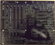
I just received the PCBs, they look in reasonable quality and arrived undamaged as far as I can see.
And they remained straight as well and not warped due to shrink wrapping, so it's looking good so far.
I will start the assembly work now, I am still waiting for the PLCC 84 pin sockets to arrive so my testing work and programming the CPLDs will need to wait at least until I have those.
And they remained straight as well and not warped due to shrink wrapping, so it's looking good so far.
I will start the assembly work now, I am still waiting for the PLCC 84 pin sockets to arrive so my testing work and programming the CPLDs will need to wait at least until I have those.
Attachments
A small update to the work on the project.
I have done a lot of work on the mainboard, the work was made more difficult by a shortage of components which I had to desolder from other mainboards.
This posed another complication because those mainboards were faulty and unstable so I needed to verify whether what I took from these boards is at least working and not defective. So I desoldered various ICs from my 5170, put in sockets and used the 5170 as a test computer to test a lot of ICs which I needed for the prototype PCB. I also used the ARC mainboard which I bought last and which is kind-of functional but not great.
I marked the "tested good" components with a small sticker so I can work from a base of known functional components in critical areas.
After having tested a good number of desoldered components, I proceeded to assemble the PCB.
I also found two 84 pin PLCC sockets in my parts box which I didn't know I have.
And I have a faulty A500 mainboard which I can borrow a third socket from.
Since the sockets from Italy seem to be taking a long time to arrive.
I made a small list of parts which were not in "stock", in other words I never ordered those and must search a long time to find them on other boards or amongst unsorted parts. So far I am managing to "piece together" the mainboard.
I received 10 CPLDs from China which are recycled parts, so I will need to first erase those before connecting them to anything, otherwise the CPLDs will be destroyed by contention I expect.
I will use the third desoldered PLCC socket on the ISA memory card with only the socket and programming header for erasing and programming all the CPLDs.
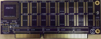
Then I will add them to the mainboard and continue to assemble the memory card. I will start first with 1MB of SRAM for testing the system.
I am expecting some small difficulty with the refresh detection routines even in case there are no other ussues. I have seen on the 5170 with the MR BIOS that it sometimes throws a refresh circuitry error, because I wired the refresh timer output to the refresh detection input on "port B" as a test to avoid those detections from happening. I understand of course that this is not "the" solution but at least on the 5170 it got me past the POST and able to test anything.
Once I have the whole system operational, I will test more and vary the logic between the refresh timer and detection input until I can get the error to completely disappear. Another method would be to change the BIOS of course but that is more complicated. If anyone has some idea about how to deal with these errors, other than creating some circuit for it, please do let me know your ideas. I first need to have the actual system running in order to be able to test further with disabling these refresh errors because that is a more complicated procedure to deal with, and I want to do the work on the actual computer it is meant for.
So it's a lot of work, I desoldered more than 1000 pins this weekend and every logic chip is taken from other AT mainboards I have tested with which had some type of problem in the past year and turned out to be unsuitable as references. So I have been testing those parts on my 5170 mainboard to make sure those are functional. I also took parts from other previous XT revision prototype boards which were not complete anyway. I soldered a lot of ICs directly into the prototype because I also have a shortage of IC sockets. It's good that I at least have a working Hakko for desoldering otherwise I cannot build this prototype for a long time while waiting for many parts.
Still a lot of soldering and searching for parts ahead, but it is progressing.
I will also need to sort out how to convert quartus codes to the Atmel programming code and procedure.
And how the Atmel software works, and I will need to make a small header adapter to suit the 5 pin JTAG header I put on the PCBs.
Only after erasing and reprogramming I dare to insert the CPLDs into their sockets.
And I will be checking the tri-state function on certain outputs to check whether that is implemented and working properly from my method in quartus.
Anyone who has expertise in this field and willing to give me some useful tips to avoid problems and speed along the project, feel free to comment here in the thread.
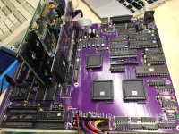
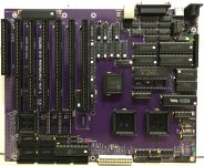
Here is a photo of the current state of the prototype mainboard PCB assembly to give you an idea/update of what it looks like now.
Kind regards,
Rodney
I have done a lot of work on the mainboard, the work was made more difficult by a shortage of components which I had to desolder from other mainboards.
This posed another complication because those mainboards were faulty and unstable so I needed to verify whether what I took from these boards is at least working and not defective. So I desoldered various ICs from my 5170, put in sockets and used the 5170 as a test computer to test a lot of ICs which I needed for the prototype PCB. I also used the ARC mainboard which I bought last and which is kind-of functional but not great.
I marked the "tested good" components with a small sticker so I can work from a base of known functional components in critical areas.
After having tested a good number of desoldered components, I proceeded to assemble the PCB.
I also found two 84 pin PLCC sockets in my parts box which I didn't know I have.
And I have a faulty A500 mainboard which I can borrow a third socket from.
Since the sockets from Italy seem to be taking a long time to arrive.
I made a small list of parts which were not in "stock", in other words I never ordered those and must search a long time to find them on other boards or amongst unsorted parts. So far I am managing to "piece together" the mainboard.
I received 10 CPLDs from China which are recycled parts, so I will need to first erase those before connecting them to anything, otherwise the CPLDs will be destroyed by contention I expect.
I will use the third desoldered PLCC socket on the ISA memory card with only the socket and programming header for erasing and programming all the CPLDs.
Then I will add them to the mainboard and continue to assemble the memory card. I will start first with 1MB of SRAM for testing the system.
I am expecting some small difficulty with the refresh detection routines even in case there are no other ussues. I have seen on the 5170 with the MR BIOS that it sometimes throws a refresh circuitry error, because I wired the refresh timer output to the refresh detection input on "port B" as a test to avoid those detections from happening. I understand of course that this is not "the" solution but at least on the 5170 it got me past the POST and able to test anything.
Once I have the whole system operational, I will test more and vary the logic between the refresh timer and detection input until I can get the error to completely disappear. Another method would be to change the BIOS of course but that is more complicated. If anyone has some idea about how to deal with these errors, other than creating some circuit for it, please do let me know your ideas. I first need to have the actual system running in order to be able to test further with disabling these refresh errors because that is a more complicated procedure to deal with, and I want to do the work on the actual computer it is meant for.
So it's a lot of work, I desoldered more than 1000 pins this weekend and every logic chip is taken from other AT mainboards I have tested with which had some type of problem in the past year and turned out to be unsuitable as references. So I have been testing those parts on my 5170 mainboard to make sure those are functional. I also took parts from other previous XT revision prototype boards which were not complete anyway. I soldered a lot of ICs directly into the prototype because I also have a shortage of IC sockets. It's good that I at least have a working Hakko for desoldering otherwise I cannot build this prototype for a long time while waiting for many parts.
Still a lot of soldering and searching for parts ahead, but it is progressing.
I will also need to sort out how to convert quartus codes to the Atmel programming code and procedure.
And how the Atmel software works, and I will need to make a small header adapter to suit the 5 pin JTAG header I put on the PCBs.
Only after erasing and reprogramming I dare to insert the CPLDs into their sockets.
And I will be checking the tri-state function on certain outputs to check whether that is implemented and working properly from my method in quartus.
Anyone who has expertise in this field and willing to give me some useful tips to avoid problems and speed along the project, feel free to comment here in the thread.
Here is a photo of the current state of the prototype mainboard PCB assembly to give you an idea/update of what it looks like now.
Kind regards,
Rodney
Attachments
Last edited:
I have fully assembled the mainboard and soldered 1MB of SRAM onto the memory card.
Of my 10 CPLDs only 4 are able to erase and program.
Possibly the JTAG pins are disabled on the other CPLDs or they are defective.
To re-enable the JTAG pins would be requiring a special programmer to do this as I understand.
But maybe they can be re-enabled in other ways, if anyone knows please let me know.
I have programmed the three CPLDs in the design and I am now testing the mainboard with the memory card and a video card.
I have also tested with a ATI Small wonder card to see if I can catch any BIOS message on the monochrome CRT which doesn't show up on VGA.
The PC is not stable yet but after certain power cycles it is functioning more already than initially.
I have found a few things so far:
- the memory decoding system works and allocates the 640KB of base memory from the first soldered 1MB or SRAM which is reported by the BIOS.
- the CPLDs appear to be doing some programmed tasks such as creating the clock pulses, decoding the RAM, BIOS ROMs and also the option ROM is probably working, when inserted I have seen the screen of XT-IDE come through
- there appears to be a level of 8 bit conversion going on according to the LED
- after a few power cycles I can see the VGA BIOS, then the MR BIOS reports a 8Mhz 80286,
640KB or RAM and that the RTC contents is corrupt(which is correct)
- sometimes a BIOS message alert was able to produce the beep sound from the speaker
- I have seen keyboard control to function a few times and was able to CTRL-ALT-DEL the computer but at that time the screen information was corrupted.
What is happening is that the CPU becomes active, loads the VGA BIOS and MR BIOS screens, and after a few seconds it stops being active.
The screen then freezes and keeps the last content. When the CPU is inactive, the data lines also are quiet.
The internal RESET line on the mainboard has been rather noisy for which the system is sensitive of course, so I added a capacitor to GND of 2,2nF near the FDC and another 470pF directly on the 82284 RESET pin. This has improved the CPU operation somewhat and it's able to run for a longer period of time before freezing. About a few seconds.
I also added a 15k resistor to GND on the PEREQ line which I have seen on other AT mainboards.
Probably this is more necessary if there is no coprocessor present.
I also replaced the two SRAMs I initially soldered just to make sure that this was not the problem.
Initially I got a lot of corrupted characters on the screen which appeared like some memory issue so I soldered a different pair of SRAMs which seemed to have fixed that character distortion problem. Now when I am able to get some screens the text is mostly readable.
I will test further to try to solve the problem where the CPU is freezing after a few seconds.
I still need to determine up to what level every part of the system is functioning and I need to verify many things.
I will try to determine in what area the instability is caused. Possibly it may also be related to the impedance of the PCB influencing the clock pulses.
So the load capacitors on the various oscillators probably need to be fine tuned more to suit the PCB.
These are typical things I have seen before with my prototype designs because the PCB impedance for example is a new variable with a new PCB layout.
Particularly I have seen where there is more GND shielding present, this will present a larger load capacitance on the clock lines.
So in that case the load capacitors may need to be lowered. This problem was considerable on my third XT revision for example.
Also I will test those ICs which I have not yet fully confirmed to be functional.
I will need to order more sockets so I can exchange ICs more easily in the future.
Another thing I need to confirm is whether the functions of tri state outputs and bidirectional outputs on the CPLDs are correctly functioning where necessary for example. When I am able to test DMA that could be one way to confirm this, and I can have a look at the waveforms on those inputs that become outputs during DMA.
The 82288 and 82284 are coming from two marginal mainboards which had a lot of issues so I will probably test with the ones from the 5170 to make sure, and then I will test the other set in the 5170 as well.
I will work on confirming more things and take a closer look at the clock lines to see if they can benefit from some lower load capacitors.
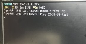
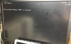
I am able to get a few BIOS screens working after a number of power cycles, I made a few screenshots of them.
So that's where I am at right now in the testing and debugging work.
The is a final issue of the POF 2 JED conversion where you can set a few parameters.
There is also a speed setting which I set to "slow" because this was said to be more stable.
Maybe later I will try the "fast" setting instead to see if this produces any change.
Also I will measure all the CPLD outputs on the scope to see if they are able to drive the circuits they are connected to.
I should probably start with the clock pulses and testing some critical ICs which have not been tested yet.
I need to find a way to test the SMD SRAMs. Probably they are best tested in my XT PC.
Kind regards,
Rodney
Of my 10 CPLDs only 4 are able to erase and program.
Possibly the JTAG pins are disabled on the other CPLDs or they are defective.
To re-enable the JTAG pins would be requiring a special programmer to do this as I understand.
But maybe they can be re-enabled in other ways, if anyone knows please let me know.
I have programmed the three CPLDs in the design and I am now testing the mainboard with the memory card and a video card.
I have also tested with a ATI Small wonder card to see if I can catch any BIOS message on the monochrome CRT which doesn't show up on VGA.
The PC is not stable yet but after certain power cycles it is functioning more already than initially.
I have found a few things so far:
- the memory decoding system works and allocates the 640KB of base memory from the first soldered 1MB or SRAM which is reported by the BIOS.
- the CPLDs appear to be doing some programmed tasks such as creating the clock pulses, decoding the RAM, BIOS ROMs and also the option ROM is probably working, when inserted I have seen the screen of XT-IDE come through
- there appears to be a level of 8 bit conversion going on according to the LED
- after a few power cycles I can see the VGA BIOS, then the MR BIOS reports a 8Mhz 80286,
640KB or RAM and that the RTC contents is corrupt(which is correct)
- sometimes a BIOS message alert was able to produce the beep sound from the speaker
- I have seen keyboard control to function a few times and was able to CTRL-ALT-DEL the computer but at that time the screen information was corrupted.
What is happening is that the CPU becomes active, loads the VGA BIOS and MR BIOS screens, and after a few seconds it stops being active.
The screen then freezes and keeps the last content. When the CPU is inactive, the data lines also are quiet.
The internal RESET line on the mainboard has been rather noisy for which the system is sensitive of course, so I added a capacitor to GND of 2,2nF near the FDC and another 470pF directly on the 82284 RESET pin. This has improved the CPU operation somewhat and it's able to run for a longer period of time before freezing. About a few seconds.
I also added a 15k resistor to GND on the PEREQ line which I have seen on other AT mainboards.
Probably this is more necessary if there is no coprocessor present.
I also replaced the two SRAMs I initially soldered just to make sure that this was not the problem.
Initially I got a lot of corrupted characters on the screen which appeared like some memory issue so I soldered a different pair of SRAMs which seemed to have fixed that character distortion problem. Now when I am able to get some screens the text is mostly readable.
I will test further to try to solve the problem where the CPU is freezing after a few seconds.
I still need to determine up to what level every part of the system is functioning and I need to verify many things.
I will try to determine in what area the instability is caused. Possibly it may also be related to the impedance of the PCB influencing the clock pulses.
So the load capacitors on the various oscillators probably need to be fine tuned more to suit the PCB.
These are typical things I have seen before with my prototype designs because the PCB impedance for example is a new variable with a new PCB layout.
Particularly I have seen where there is more GND shielding present, this will present a larger load capacitance on the clock lines.
So in that case the load capacitors may need to be lowered. This problem was considerable on my third XT revision for example.
Also I will test those ICs which I have not yet fully confirmed to be functional.
I will need to order more sockets so I can exchange ICs more easily in the future.
Another thing I need to confirm is whether the functions of tri state outputs and bidirectional outputs on the CPLDs are correctly functioning where necessary for example. When I am able to test DMA that could be one way to confirm this, and I can have a look at the waveforms on those inputs that become outputs during DMA.
The 82288 and 82284 are coming from two marginal mainboards which had a lot of issues so I will probably test with the ones from the 5170 to make sure, and then I will test the other set in the 5170 as well.
I will work on confirming more things and take a closer look at the clock lines to see if they can benefit from some lower load capacitors.
I am able to get a few BIOS screens working after a number of power cycles, I made a few screenshots of them.
So that's where I am at right now in the testing and debugging work.
The is a final issue of the POF 2 JED conversion where you can set a few parameters.
There is also a speed setting which I set to "slow" because this was said to be more stable.
Maybe later I will try the "fast" setting instead to see if this produces any change.
Also I will measure all the CPLD outputs on the scope to see if they are able to drive the circuits they are connected to.
I should probably start with the clock pulses and testing some critical ICs which have not been tested yet.
I need to find a way to test the SMD SRAMs. Probably they are best tested in my XT PC.
Kind regards,
Rodney