• Please review our updated Terms and Rules here
  • From now on we will require that a prefix is set for any items in the sales area. We have created regions and locations for this. We also require that you select a delivery option before posting your listing. This will hopefully help us streamline the things that get listed for sales here and help local people better advertise their items, especially for local only sales. New sales rules are also coming, so stay tuned.

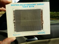
Midwest 1958 Mated-Film Memory Array 1024 bits Univac Sperry Rand Prototype - ? $$

Covers: North Dakota, South Dakota, Nebraska, Kansas, Minesota, Iowa, Missouri, Wisconsin, Illinois, Michigan, Indiana and Ohio

wala0003

New Member
Joined
Sep 19, 2023
Messages
2
Delivery Options
International Shipping

Very unique piece of computer history.


Bought it at a MN garage sale. Curious if it has any real value.

What I could find:

https://www.computerhistory.org/collections/catalog/X93.82


Film Memory Development Work at Univac by Dick Petschauer.

This work started at Univac Research Dept under Dr. Sid Rubens in about 1954. I started in 1956 in the Memory Engineering Department. Specifically, I was assigned to do the circuit design in Dr Ruben’s group working for Dr. Art Pohm. Dr. Pohm was heading up a project to make an experimental memory. After completing this we got a contract from the Air Force Ballistics Missile Division. They wanted a non-destructive read out memory to replace the drum memories in on-board guidance computers.

The Air Force was concerned about the reliability of the mechanical drum memories. The ferrite core memories used at that time had to be cleared every read cycle in order to determine if they stored a one or zero, after which the data was rewritten. For program storage there was a concern that transient errors could result in permanent changes in the memory. While the first thin film memories also needed rewriting each cycle, other ways to use them had the promise of providing non-destructive read out, or “NDRO”, operation.

The initial approach for NDRO used the technique of “reversible rotation“. A magnetic read field is applied perpendicular to the normal direction of magnetization which produces a small positive or negative signal depending on whether a one or zero was stored. However, for a number of reasons, operation was sometimes unreliable and many readouts and could cause partial demagnetization and loss of output signal. In the middle of the Air Force contract, we changed directions and adopted the “Bicore” approach, which used a two layered film with a “strong” layer and a “weak” layer. Writing was accomplished by switching the strong layer and its external magnetic field would force the weak film to a state that would close the flux path. Reading was done by clearing the weak layer with a smaller current and sensing whether it switched. The read current did not change the state of the strong layer. After reading, the strong layer would restore the weak layer.

This approach proved highly successful. The first test memory of 288 bits was built and described in a detailed internal paper written on July 29, 1960. This was followed by the construction of a larger 1024 by 36 bit and this was reported at the 1961 Western Joint Computer Conference in Los Angeles. All previous film memories were much smaller and were in a single plane. This memory was in a 16-plane stack, an industry first.

Improvements came rapidly. In May of 1962 Univac reported on a 166,000 bit Bicore memory. This was the basis for the Univac ADD airborne computer. It used both an NDRO film memory and a fast smaller DRO film memory in a very small 1.1 cubic foot computer, including power supplies. This was before the advent of the integrated circuits and used separate transistors, diodes, resistors and capacitors for all the circuits. The components were stacked a 3D “cordwood” style in small welded packages.


20141026_122704_Vincent Ave S.jpg
 
I don't, the substrate seems to be some sort of glass like material. It's only about 2"x2". I could weigh it if you need.
 
Welcome to the forums. Yes, a very interesting piece of history. I like reading about things I don't know about. Thanks.
 
I don't, the substrate seems to be some sort of glass like material. It's only about 2"x2". I could weigh it if you need.
I am really curious if you could drive it with e.g. an Arduino or something - any idea how it connected to a computer?
 
I believe that the 1107 used thin-film memory, but that never made it to the 1108. Pretty much an evolutionary dead-end, unless you count, say, bubble memory or FRAM. I guess UNIVAC was always on the lookout for interesting memory technology; they used plated-wire memory on the 1110.
 
Last edited:
The fact that the memory plane is on a PR display card makes me wonder if it wasn't a manufacturing reject. cf the Intel CPU chip keyfobs--real chips in there, not bonded out, likely failures in the initial probe.
 
The Computer History Museum in Santa Clara has one of these exact things in their collection according to their website… although their copy is in a little worse shape. (The glue holding the slide to the card has given up.)

I second that there’s a very good chance this thing is nonfunctional. Sure, I suppose you might hand out samples at trade shows or whatever, but the working ones aren’t going to be glued to sheets of cardboard.
 
Re: the key fob thing, somewhere in the garage I have a promotional binder from Motorola I found in an eWaste bin that has about a dozen real CPU chips on the front cover, ranging from tiny microcontrollers to PowerPC CPUs. I would certainly guess they’re all duds, although maybe they didn’t care with the smaller/cheaper ones.

Unfortunately the glue gave up and most of the dies are rattling around loose under the plastic lamination, so if I want to actually know which is which I’d have to do a bit of research. ;)
 
The fact that the memory plane is on a PR display card makes me wonder if it wasn't a manufacturing reject.
I also agree that it is a very period-correct thing to have done.
Unfortunately the glue gave up and most of the dies are rattling around loose under the plastic lamination, so if I want to actually know which is which I’d have to do a bit of research.
...or you could make an online game out of it by taking pictures of them and having people do the work for you as a challenge. ;)
 
Re: the key fob thing, somewhere in the garage I have a promotional binder from Motorola I found in an eWaste bin that has about a dozen real CPU chips on the front cover, ranging from tiny microcontrollers to PowerPC CPUs. I would certainly guess they’re all duds, although maybe they didn’t care with the smaller/cheaper ones.

Unfortunately the glue gave up and most of the dies are rattling around loose under the plastic lamination, so if I want to actually know which is which I’d have to do a bit of research. ;)

My 386/486 key fob is cast resin. Nothing rattling there--I suppose I could make it rattle if I gave it a few good whacks with a sledgehammer....
 
Back
Top