• Please review our updated Terms and Rules here

6809 and Dynamic Address Translation (DAT)

ncherry

Experienced Member
Joined
Mar 4, 2018
Messages
112
Location
Monroe Twp, NJ
I have some documents on the SWTPC DAT (Dynamic Address Translation) but I don't quite understand it. I understand that you write something to 0xFFFx and it selects one of 0xFF 4k blocks but the circuit I see reads the address lines and not the memory locations. Does anyone have a decent explanation of it's operation? Such that I can write to 0xFFFx and set the ram at xxxx to be block 0xXX.
 
Firstly its not clear when you say it "does not read the memory locations" if you mean the main memory locations, or the memory at 0xFFFx? I will assume you mean 0xFFFx. Well that is true, it never reads the translate RAM using those addresses. Reading those addresses access the system ROM. If it didn't the system wouldn't even reset. The DAT translate memory is only visible @ 0xFFFx on a "write" cycle.

So how does it work. OK, well lets look at what the circuit is called. Its "Dynamic Address Translation". So the translation happens "Dynamically" that is as the CPU is running a program for each memory access.

As you say the DAT RAM is addressed by the address line, the top four in fact. So for example when the CPU tries to access location 0x3000 the top four address lines do not get passed out onto the SS50 BUS. Instead they are used to address the DAT RAM. As the are "0x3" they read the location you wrote to at address 0xFFF3. The content of this location is used to generate a new 20 bit address that is passed out on the SS50 bus. It would be nice say that if the RAM had 0x03 stored in it, then for example "0x367F" would be "translated" and passed to the bus as 0x0367F but in fact some inversion takes place. See the doc below for details. The address is now a 20 bit address (5 hex digits) because the DAT RAM is 8-bits wide. This allows use to have up to 1Mb of RAM in a system but of course programs only see 64k at any one time.

The Corsham Technology CPU board manual which you can download from here:-

http://www.corshamtech.com/product/ss-50-6809-cpu-board/#

has a good description of how to ue it. Hope this helps. I had to read that manual to understand how it works...
 
Huge thanks Dave. That helped a lot. I was staring at the schematics of different MP-09 boards and was having trouble reading them. I think I over analysed them last night. Your explanation and the docx file clears it up. So I see now that any one process can only see a 64k window of the available memory.
 
No problems. I have a couple of SWTPC 6809 systems so wondered how it worked. I found it hard to get an answer and was about to go delving into the documents when I found the Corsham document which is really clear.
 
A similar system is used for the TI9900 series using the 74LS612 IC to map 4 bits of memory address to 12. Also used in the IBM PC series to extend the 64K addressing of the 8237A DMA controller (which has only 16 bits of address) to the full installed memory, albeit with restrictions (e.g., you can't cross a 64K memory boundary--data accesses will "wrap" back to the beginning of the 64K block). Think of it a type of bank-switching.

We used the same scheme back in the day using a 64x9 bipolar RAM on an 8085 to get another few bits of address space. Note that insertion of a memory mapper or MMU does carry an access time penalty, which is why we resorted to a bipolar RAM (power hungry, but faster than CMOS/NMOS).

Here's an article about using a 74LS612 with a 6502 to expand memory addressability.
 
Last edited:
When I was thinking of building the 6809 board, I spent a lot of time trying to make sense of the SWTPC DAT circuit. Frankly, I wasn't convinced it ever really worked, so I did some very slight mods to it. My suspicion is that nobody had enough memory boards to go beyond the 16 bit address bus, so the extended address area was never tested.

While playing with the circuit, only 74LS189s were the right speeds, unlike the SWTPC schematic which shows S versions. The pull-up on R/W is definitely necessary.

Anyway, while trying to understand how it worked, I wrote out a description which eventually ended up in the user manual for the Corsham Tech board.

Bob
(Corsham Tech)

Bob,

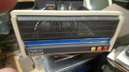
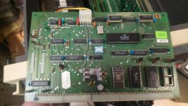
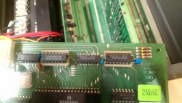
Well that made me curious. Firstly as the DAT is always active, it doesn't matter if you have more or less than 64K, the mapper still maps the 16 4K pages. Secondly I looked at one of my boards which is modded for 2Mhz. I suspect it ran UNIFLEX rather than plain FLEX so the DAT was used, but I can't be sure I have no history for the systems. It definitely has 74S189 chips. There is an assortment of date codes on it the chips on it. Most are 81xx so most likely built in 1981. Sorry the case photos are a bit naff, I will try for some better ones tomorrow if you are interested.

Dave

DSC_2855.jpg
DSC_2857.jpg
DSC_2861.jpg
 
Dave's explanation and your (Bob's) document have been very helpful. One of the issues I had was the real SWTPC schematics are hard to read and I was confused by how the DAT worked. I hadn't looked at your document or schematics before hand. Now I have and I've now been able to switch bank 8 into $4000 while in sbug (I'm using the emulator right now, real thing later). :)
 
True, but the upper four address bits probably weren't used for a while as most systems didn't have more than 64K. The original schematics from SWTPC didn't seem to make sense, but then they issued some written instructions how modifications they made. The schematics on the web don't show those changes. I also had some other unique issues on my board since it had 128K on the board instead of all memory being off-board. One of my most difficult problems was trying to find why accesses to the DAT registers would sometimes modify low memory! Debugging was rather frustrating.

BTW, the 6809 board was the most unpleasant board I developed. It took months and the DAT logic was not easy to get timing right. I've toyed with the idea of making a small CPLD that does the DAT logic so it can be used as a plug-and-play module on other boards.

Bob
 
True, but the upper four address bits probably weren't used for a while as most systems didn't have more than 64K. The original schematics from SWTPC didn't seem to make sense, but then they issued some written instructions how modifications they made. The schematics on the web don't show those changes. I also had some other unique issues on my board since it had 128K on the board instead of all memory being off-board. One of my most difficult problems was trying to find why accesses to the DAT registers would sometimes modify low memory! Debugging was rather frustrating.
Yes, I could see the onboard RAM being difficult. It's good to know that it wasn't just me that was having trouble with reading the schematics (not yours, MP-09 V2)

I can now say I understand what the DAT does and demonstrated it by modifying memory in the SWTPC emulator. But don't ask me to draw it. I might be able to explain it. ;-)

My current projects are many (way too many, some not even related to computers - yikes!). The emulator lets me get my tool chains and assembler knowledge back in order. I'm hoping to get my Sardis ST2900 fully operational with OS-9 Level 2 by the end of the year and I am considering getting a full HCS II (Home Automation) system up for a presentation next year. Let's see what the year brings first.
 
Back
Top