• Please review our updated Terms and Rules here

80188 Address Decoder for TMS9918A Help.

80186 Enthusiast

Experienced Member
Joined
May 18, 2023
Messages
53
Here's a schematic I've made for an address decoder for a TMS9918A Video Display Processor. In this Post, I'll go over how this Address Decoder Works .
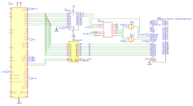
Schematic_80188 2 VDP_2023-06-06.png
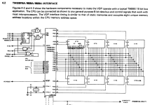
I've based this address decoder off of schematics in the Datasheet (I'll put those schematics at the bottom of this post) for the TMS9918A. The main component of this Address Decoder is a 47LS138 Decoder/ Demultiplexer IC.
The I have Enable Pin G1 tied to 5v, and Enable Pin G2A tied to GND. Enable Pin G2B is connected to CPU pin PCS0. PSC0 is used to put the VDP on the CPU's memory Map, this signal will be programmed to be pulled low whenever the CPU needs to communicate with the VDP. (74LS138 truth table below)
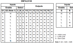
Screenshot (131).png
The VDP requires specific addresses (or ports as the VDP datasheet says) to let it know when the CPU is Writing, Writing an Address, reading from VRAM and Reading the VDP Status Register. So I referenced the Datasheet for what Ports I wanted to use and which address pins I needed to use. So I converted each Port/ Addresses I needed to use and created the following table:
A19 A18 A17 A16​
A15 A14 A13 A12​
A11 A10 A9 A8​
A7 A6 A5 A4​
A3 A2 A1 A0​
0 0 0 0​
1 0 0 0​
0 0 0 0​
0 0 0 0​
0 0 0 0​
0x08000: Write Data to VRAM
0 0 0 0​
1 0 0 0​
0 0 0 0​
0 0 0 0​
0 0 1 0​
0x08002: Write Address to VRAM
0 0 0 0​
1 0 0 0​
0 0 0 0​
0 0 0 0​
0 1 0 0​
0x08004: Read Data from VRAM​
0 0 0 0​
1 0 0 0​
0 0 0 0​
0 0 0 0​
0 1 1 0​
0x08006: Read VDP Status

So I need Address Pins A15, A2 and A1. By using those Address Pins as the Select Input pins in the 74LS138 in the following order:
  • A15 => C
  • A2 => B
  • A1 => A
If you look at the Truth Table for the 74LS138, Whenever Select Input Signal is High, the lower 4 bits of the output side is used. And only 1 Output can be Low at a Time, So the following List is created:
  • Y4 low = Write Data to VRAM (A15 High: 0x08000)
  • Y5 low = Write Address to VRAM (A15, A1 High: 0x08002)
  • Y6 low = Read Data from VRAM (A15, A2 High: 0x08004)
  • Y7 low = Read VDP Status Register (A15, A2, A1 High: 0x08006)
The Outputs of the Decoder are connected to the inputs of a 3 input AND gate, the VRAM Write command port Gate also has the CPU Write Strobe. The VRAM/ VDP Read command port Gate has the CPU Read Strobe. This is Done to treat these VRAM/ VDP Read and Write Commands as Memory Read and Write sequences and enable the AND gates when the Read or Write Strobe goes LOW. so the 16k of VRAM will be in the CPU's memory Map as a list of addresses the VDP is compatible with. the CPU will access VRAM through the VDP by using the Data Bus, as Intended by Texas Instruments.

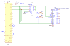
That's it for this post, as always, any help and advice will be thanked and appreciated in Advance! Here are are the schematics from the Datasheet as I mentioned earlier in this Post!
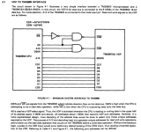
Screenshot (133).pngScreenshot (134).png
 
The VDP requires specific addresses (or ports as the VDP datasheet says) to let it know when the CPU is Writing, Writing an Address, reading from VRAM and Reading the VDP Status Register. So I referenced the Datasheet for what Ports I wanted to use and which address pins I needed to use.

Ball that all up and throw it out the window. The addresses you’re referring to were specific suggestions for interfacing it with a TMS9900 CPU.

If you’re using a PCS* signal from the 80188 you don’t need an address decoder on at address lines at all; that’s kind of the point. This chip, according to my recollection, only has two bidirectional ports, IE, a command/status port and a data port. Those are selected with the “mode” line; connect that directly to A0 and you’ll have those two functions on consecutive byte addresses starting at whatever you program the PCS line for.

The only other thing you need is a pair of AND gates to combine PCSx separately with RD and WR to produce the combined CSR and CSW signals.
 
The other thing you need to check is the RESET line. From the looks of your schematic this appears to be active HIGH for the CPU and active LOW for the video chip.

As Eudi has already said, just because there is a load of external logic in the data sheet doesn't mean you actually need it with a CPU with an integrated (and programmable) address decoding engine!

Dave
 
connect that directly to A0

Just to be clear, this is the demultiplexed A0 you should already have available from the address latch you put in front of your memory chip. You don’t need a separate address latch on ALE for every device, depending on the chip family you use for the address latches you should be fine fanning it out to a couple dozen things.
 
Ball that all up and throw it out the window. The addresses you’re referring to were specific suggestions for interfacing it with a TMS9900 CPU.

If you’re using a PCS* signal from the 80188 you don’t need an address decoder on at address lines at all; that’s kind of the point. This chip, according to my recollection, only has two bidirectional ports, IE, a command/status port and a data port. Those are selected with the “mode” line; connect that directly to A0 and you’ll have those two functions on consecutive byte addresses starting at whatever you program the PCS line for.

The only other thing you need is a pair of AND gates to combine PCSx separately with RD and WR to produce the combined CSR and CSW signals.

I have 3 Questions:
  1. Will the address decoder I've designed work?
  2. Will using a 3 Input AND gate work for what I need?
  3. Again, Why didn't I think about that? (this is why I always come to this forum for help.)
 
Last edited:
Will the address decoder I've designed work?

Sort of, but it’s completely redundant and the resulting mapping would be goofy and unnecessary.

The decoder in the manual is for a 16 bit CPU that only supports 16 bit operations and memory mapped I/O, and the example wastes *half of the memory space* to decode this one peripheral. (Another thing that I think might have confused you is the 9900 numbers its address lines backwards…) The 9900 also has other goofy quirks you don’t care about on the 80188; the reasons this design puts the reads and writes on different addresses is because the 9900 always does a read before a write, always, and that would confuse the VDP. Their circuitry does the alternate addressing to filter that out.

The only thing your circuit would accomplish in an 80188 design where you’re using a PCS line is A: separate reads and writes onto separate addresses which, again, you don’t need, and B: that line to A15 is completely unnecessary and all it would do is prevent the PCS select from working unless it was programmed to activate at an address in the top half of the 16 bit I/O port range.


Will using a 3 Input AND gate work for what I need?

I stand corrected (apparently I hadn’t had my coffee yet), it’s actually a pair of two input ORs, not ANDs you need. (An OR isn’t zero unless both inputs are zero. You don’t want CSR and CSW to see a zero unless RD+PCSx or WR+PCSx are both zero, respectively.)
 
I am a little confused about the signal naming myself. Are the signals really RD and WR or /RD and /WR? It makes a complete difference.

Eudi's covered pretty much the same as I would have done.

The only thing I would say, is that by eliminating the address lines that are '0' you have effectively changed them into "don't care' or 'X', and this was not the intent of the logic on the data sheet - although the /PCS line would make up for that deficiency.

Yes, the ordering of the bit numbers has really caught you out there! The 'high numbered' address lines are really low address lines.

Dave
 
am a little confused about the signal naming myself. Are the signals really RD and WR or /RD and /WR? It makes a complete difference.

I need to be better about including a / or * for the active-low signal names; chalk it up to sheer laziness. :( Anyway, it looks like all of /RD,/ WR, /CSR, /CSW, and /PCSx are active lows so a single 74LS32 or the like should be all you need to interface this monster.(*)

(Programmable chip selects are actually pretty neat, aren't they.)

(* EDIT: Other than possibly the issue with inverted RESETs? I also haven't dug into how the 9918 uses interrupts, you might need to double-check that you can connect that straight up or if that needs any massaging.)
 
Last edited:
I have 3 Questions:
  1. Will the address decoder I've designed work?
No, it won't work. The reason is: WR and RD are active-low write and read strobes. The way the 3-input AND gates U4.2 and U4.3 are connected now, they are performing a logic-OR function of the active low signals.
As a result the TMS9918A will have its !CSW write input activated whenever WR is active (low) or when either the Y4 or Y5 outputs of the '138 are active. Similarly, the TMS9918A will have its !CSR read input activated whenever RD is active (low) or when either the Y6 or Y7 outputs of the 74LS138 are active. This is definitely not what you want because the TMS99xx will be activated by every bus read or write.
  1. Will using a 3 Input AND gate work for what I need?
No. You actually want a 2-input OR gate here. Sounds counter-intuitive but by De Morgan's laws, an OR gate performs an AND function with active-low inputs and an active-low output. Yes, you could use a 3-input OR here but, as others have mentioned above, it's not necessary to decode two different addresses for a read and another two for a write. Only a single address bit is needed to keep accesses to the TMS9918A register space and video RAM space separate, and that's what the MODE pin is for.

I would do the following using a 74LS32 quad OR gate:
pin 1 of the 74LS32 connected to 80188 WR/
pin 2 of the 74LS32 connected to 80188 PCS0/
pin 3 of the 74LS32 connected to TMS9918 !CSW
pin 4 of the 74LS32 connected to 80188 RD/
pin 5 of the 74LS32 connected to 80188 PCS0/
pin 6 of the 74LS32 connected to TMS9918 !CSR
of course, also +5V and GND to the 74LS32.

The address latch A0 bit connects to the TMS9918A MODE pin as you have it. Also as Eudi mentioned, if there's already another address latch in the system, use that one to grab A0.

One more issue:
the 74LS245 transceiver is enabled on every bus cycle as it's connected now. Every DEN active will enable the 74LS245. If this system is not large then the 74LS245 isn't necessary. Just connect 80188 AD0 to TMS9918A CD7 and so on through AD7 connect to CD0. I see by the way it's connected now you already know that TI numbers their bits differently than Intel.

Oh, also as I think Daver2 mentions: the RESET output of the 80188 is active-high and the !RESET input of the TMS9918A is active-low, so you need an inverter between them.

  1. Again, Why didn't I think about that? (this is why I always come to this forum for help.)
:)
 
it's not necessary to decode two different addresses for a read and another two for a write. Only a single address bit is needed to keep accesses to the TMS9918A register space and video RAM space separate, and that's what the MODE pin is for.

That's one perhaps ironic thing about the TI9918A; the datasheet uses interfacing to a TMS9900 as an example, but the chip, other than its backwards labels, seems like it was tailor made to work with an 8080/Z80-style bus (which of course the 80188 is pretty close to). You almost couldn't ask for a better fit.
 
No, it won't work. The reason is: WR and RD are active-low write and read strobes. The way the 3-input AND gates U4.2 and U4.3 are connected now, they are performing a logic-OR function of the active low signals.
As a result the TMS9918A will have its !CSW write input activated whenever WR is active (low) or when either the Y4 or Y5 outputs of the '138 are active. Similarly, the TMS9918A will have its !CSR read input activated whenever RD is active (low) or when either the Y6 or Y7 outputs of the 74LS138 are active. This is definitely not what you want because the TMS99xx will be activated by every bus read or write.

No. You actually want a 2-input OR gate here. Sounds counter-intuitive but by De Morgan's laws, an OR gate performs an AND function with active-low inputs and an active-low output. Yes, you could use a 3-input OR here but, as others have mentioned above, it's not necessary to decode two different addresses for a read and another two for a write. Only a single address bit is needed to keep accesses to the TMS9918A register space and video RAM space separate, and that's what the MODE pin is for.

I would do the following using a 74LS32 quad OR gate:
pin 1 of the 74LS32 connected to 80188 WR/
pin 2 of the 74LS32 connected to 80188 PCS0/
pin 3 of the 74LS32 connected to TMS9918 !CSW
pin 4 of the 74LS32 connected to 80188 RD/
pin 5 of the 74LS32 connected to 80188 PCS0/
pin 6 of the 74LS32 connected to TMS9918 !CSR
of course, also +5V and GND to the 74LS32.

The address latch A0 bit connects to the TMS9918A MODE pin as you have it. Also as Eudi mentioned, if there's already another address latch in the system, use that one to grab A0.

One more issue:
the 74LS245 transceiver is enabled on every bus cycle as it's connected now. Every DEN active will enable the 74LS245. If this system is not large then the 74LS245 isn't necessary. Just connect 80188 AD0 to TMS9918A CD7 and so on through AD7 connect to CD0. I see by the way it's connected now you already know that TI numbers their bits differently than Intel.

Oh, also as I think Daver2 mentions: the RESET output of the 80188 is active-high and the !RESET input of the TMS9918A is active-low, so you need an inverter between them.


:)
Schematic_80188 2 VDP_2023-06-14.png
Here is the revised 80188 CPU => TMS9918 VDP Address decoder and Interface schematic!
Thank you for this better address decoder!
 
That's looking better now.

Don't forget that U2 is not necessary - as it is part of the low address latch for the ROM/RAM sub-system.

You really should get used to identifying the active LOW logic signals in some way (e.g. you have RESET and RESET - one is active HIGH and the other is active LOW).

You need to check the interrupt line from the video processor to the CPU to ensure (a) it us not open collector and (b) one of the signals is not inverted.

Dave
 
...or a bar/macron over the signal name (I'd try it here, but BBCode doesn't seem to support a combining macron.) A minus after the signal name is too easy to miss. Another way is to prefix the signal name with an "N"; e.g. NRESET--that's my least favorite way. An older technique is to show the device with a bubble on the signal line, so that it's obvious that it's a negative-true pin.
 
One of the things that I find slightly annoying in modern schematics is the lack of recognition that if you're dealing with negative logic, the basic function of a gate is different and needs to be shown as such.
and-or.gif
 
One of the things that I find slightly annoying in modern schematics is the lack of recognition that if you're dealing with negative logic, the basic function of a gate is different and needs to be shown as such.
and-or.gif
How does a Negative Inverter work?
 
Look where the bubble is. A positive inverter has the bubble on the output; i.e. taking a positive-true signal and turning it into a negative-true one. For an inverter operating on negative-true logic, the bubble is at the input side of the inverter--lack of an output bubble says that the logic becomes positive true.

Easy peasy. It's becoming uncommon to find that level of rigor in modern schematics--apparently, you're supposed to be able to figure out the polarity of the signal through haruspex or something.

Augustus De Morgan would be proud of you.
 
Easy peasy. It's becoming uncommon to find that level of rigor in modern schematics--apparently, you're supposed to be able to figure out the polarity of the signal through haruspex or something.
Looking for spots on the entrails is a good portion of the job. Indicating edge vs level triggering, also a lost art.
 
Back
Top