80186 Enthusiast
Experienced Member
- Joined
- May 18, 2023
- Messages
- 53
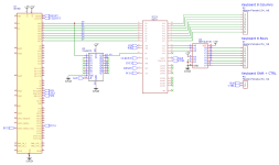
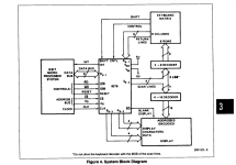
In my last post, you guys helped me to create a schematic that represents how an 80188 should interface and connect to a TMS9918A VDP. For the last main component of this prototyping project, I need a Keyboard Controller. As I stated before, I'm not going for a DOS Compatible Computer, nor do I want a computer that requires an external PS/2 Keyboard, I want this computer to have a built-in Keyboard like a Commodore Pet, Vic 20, 64, and the Apple II. This computer will be running an OS a friend and I will develop. Even though the schematic I'll show has a 74LS573, The computer itself will only have 1. The schematic just shows the CPU to Keyboard Controller connections. Speaking of that schematic ...

Here it is. I'll list my concerns in a list below:

That's it for this post, After I make an improved schematic, I'll create a schematic that represents the whole prototyping computer. Prototyping as in developing the essentials for my system, as In testing keyboard layouts and graphics related things. the first Program I'd like to make is just having an invisible grid, and whatever Letter or Number I typed pop up on the screen, and the next Letter or Number I type pop up next to the previous one.
Any help and Advice will be thanked in advance!

Here it is. I'll list my concerns in a list below:
- Latched Address Pin A0 is used for the TMS9918A, it's also used for the 8279 Keyboard controller. Should I use a different address Pin if there will be conflicts? The User Eudimorphodon said in a Previous Post of mine "depending on the chip family you use for the address latches you should be fine fanning it out to a couple dozen things."
- I've read the AP-186 Intro to the 80186 Book (in PDF form) about the Interrupt Controller and how Interrupt Requests work. However, is INT3 the only IRQ pin, or are any of the 4 INT pins able to act as IRQ inputs? I know the INT pins can't switch between detecting different kinds of Interrupts, but is INT3 the only pin that's intended to be used for an IRQ signal?
- Is there a need to have some sort of enable logic for the 74LS138 that's needed to decode the 8 Keyboard Rows?

That's it for this post, After I make an improved schematic, I'll create a schematic that represents the whole prototyping computer. Prototyping as in developing the essentials for my system, as In testing keyboard layouts and graphics related things. the first Program I'd like to make is just having an invisible grid, and whatever Letter or Number I typed pop up on the screen, and the next Letter or Number I type pop up next to the previous one.
Any help and Advice will be thanked in advance!
