Great info Dave thanks!!
So yes I would love to learn how to swap the banks.
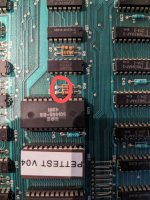
Also on changing UA11 what's the best practice? Cut the legs, or desolder gauze?
Finally do I buy a standard 4116 ram chip from eBay or something more specialised?
Thanks Andrew
De-solder wick or gauze is not too helpful clearing the plated through holes, sometimes it will, other times not.
The board has two sides, the component side and solder side:
Once the IC pins are cut close to the IC body and the body removed, you can heat the solder side of the pcb and the pin/pad, make sure to wait until the solder is fully melted and withdraw the pin from the hole on the component side of the board. To do this and have access to both sides of the board simultaneously, it is often easier to position the board vertically. Don't pull on the pin while the solder is partially heated or you will likely rip pads/tracks off the pcb. Heat & force can cause the pads & tracks to separate from the pcb.
(some people attempt removal of the IC pin from the component side of the pcb only by heating the pin and pad there, it can work, but sometimes at the factory the original solder did not flow fully down the the hole and onto the top pad on the component side. If this is the case it can be hard to transfer heat down the hole, especially with aged pcb's where the surface has oxidized, so it is always better to apply the soldering iron to the pcb solder side not the component side)
If the solder is heavily oxidized and grey looking, you can add fresh solder first.
Then after the pin is removed, add some fresh solder to the pad and hole on the solder side of the board, the fresh flux helps solder removal by the sucker.
A single shot hand held solder sucker is fine, melt the solder on the pad and hole (on the solder side) and quickly place the nozzle over the pad and deploy the sucker. If the hole does not clear, add fresh solder and repeat. Then clean up the residual flux with a cue stick and some IPA or similar pcb cleaner. Inspect everything very carefully before you solder in the IC socket. I would recommend a dual wipe socket, they are easier to remove if damaged than a machined pin type and their pins can also be removed one by one if required unlike a machine pin type. The machine pin type are much more difficult to de-solder.
and it pays to use good quality Ersin Multicore or Loctite (in the USA) 5 flux core 60/40 Tin Lead solder . There are a lot of cheap and nasty solder products out there which have poor fluxes in them. Don't use Lead free solder.
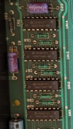
Also, you could consider getting a 4116 DRAM tester. I have tried some, one did not work properly and reported chips were defective when they were not. However, one type I bought was very good and accurately reported all chips:
Find many great new & used options and get the best deals for The Mini 4116 DRAM Tester at the best online prices at eBay! Free shipping for many products!
www.ebay.com
Most of the ebay 4116's I have bought are fine, TI, Motorola, Siemens brands etc.
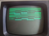
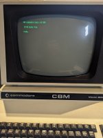
 . Will hopefully have a pettester this week so will update you!