• Please review our updated Terms and Rules here

Commodore PET problem

The simplest way to use the NOP generator is in conjunction with an oscilloscope.

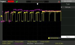
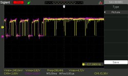
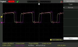
Address line A0 from the CPU should be oscillating at 250 kHz. Address line A1 from the CPU should be oscillating at half that frequency (125 kHz) and so on down to address line A15.

The same should be true on the 'other side' of the '244 address buffers.

In fact, you should be able to check the address lines are functioning correctly all the way to the ROMs and the DRAM address multiplexers using this technique. Check the two ROMs at the extremes of the block of ROM devices (it has been known for tracks to fail partway along). If the ROMs are in sockets (yours probably are not) it is prudent to check all of the ROM device address lines (just in case of an IC socket fault). Laborious, but it does identify the issue (in the case of an address pin of course)

You can also check the '154 4:16 address decoder. But more of that later if these tests checkout OK.

Of course, if the previous post works OK, you can rule out the ROMs and we can concentrate on the DRAM address multiplexers.

I am on holiday at the moment, so only limited access to schematics and other documentation...

I will have a look at your PETTESTER RAM fault displays when I get back from my (long) walk...

Dave
 
Last edited:
Yep did the NOP test to the roms and the dram multiplexers. All good.

I am working on changing the romulator to accept different memory/ram configurations so i can test just the ram or rom. I have to reprogram it to do that but that is being difficult as install apio oss-cad-suite isn't working (file not found). Have to work around that tomorrow. I am also missing two of the default roms (ramtester.bin and testromv2.out) which the faqs states you need before you can reprogram the romulator. Can't find them online.

Anyways, still can't make out the pettest output.
 
I am seeing two (2) different patterns presented. This (to me) implies it isn't a hard fault. I would try a couple more times powering on to see if a pattern starts to emerge.

Whose ROMulator did you buy?

The two I know of permits you to test ROM and RAM separately...

Dave
 
I see previously you state that the patterns generally fall into the two categories you showed.

There are still plenty of tests we can do on the DRAM interface with the NOP generator yet...

The next thing to check with the oscilloscope is the DRAM refresh addresses at the DRAM address multiplexers.

I am guessing you have Bitfixer's ROMulator?

If the characters are 'flickering' in the dotted area, this indicates to me that this is not a 'hard' fault (e.g. a stuck address or data line) more like a floating pin - or a DRAM that is just not working. The data that is being readback is varying.

Dave
 
Last edited:
I bought he bitfixer one. From my understanding, and looking at the memory map file, all the dip switch setting do is change the rom but still use the fpga ram. I could be mistaken as last night I was a bit sleep deprived.

I did find those missing .rom files in the git repo (really was falling asleep at that point). Still can't install that oss-cad-suite. According to a Google search I am not not the only one that has had this problem recently. I tried installing it manually but anyways.... I will figure it out after work.

I will look at the DRAM refresh addresses after work. Anything in particular I should look for?

Ya I figure it is two separate faults. The one fault that alternates bad every 4 addresses tends to be the most common state it is in. However, if you look at the screen shot you can see the address error at 7E & FE persist no matter what state it is in. So that part of it is for sure a consistent problem.
 
Yes, signals RAn should be oscillating away on the address multiplexers. RA1 should be 500 kHz and each higher Refresh Address line should be half the frequency of the previous one.

Dave
 
Sorry must be a slight communication issue there! I already mentioned I tested the inputs (RA1, RA2 etc...) and got the correct address values (the frequencies halving) on the multiplexers on a post a couple of days ago so I thought with your more recent post you were talking about the outputs (which are a chaotic mess).
 
We have RAn and BAn signals.

BAn signals are buffered addresses and start at 250 kHz for BA0.

RAn signals are refresh addresses and start at 500 kHz for RA1 (there is no RA0).

You did say that you checked and there were signals present - but I am more interested that you have the 'correct' signals on the buffer inputs rather than something that is present but not correct.

Dave
 
They are all correct BA0 starting at 250kHz and halving as you go down the BA Address lines and RA1 at 500kHz and halving as you go down the RA address lines
 
Excellent.

So, with the NOP generator nopping away (...) what do you see on the /RAS0, /CAS0 and /CAS1 signals?

You should see a /RAS0 pulse without a corresponding /CASn signal - this corresponding to a refresh cycle. This should also correspond to the buffer being enabled to gate the RAn signals onto the DRAM chip address lines.

You should also see a burst of activity on /CAS0. Each /CAS0 pulse should be preceded by a /RAS0 pulse. The /RAS0 signifying that half of the BAn signals have been passed to the DRAM chip and the /CAS0 signifying that the other half of the BAn signals have been passed to the DRAM chip.

You should see a bunch of activity on /RAS0 and /CAS0 (lower block of 16K RAM) followed by a bunch of activity on /RAS0 and /CAS1 (upper block of 16K RAM). Then there should be a gap in time (/RAS0 refresh cycle only - no /CASn signals) as the CPU addresses the upper 32K (video RAM, ROM and I/O).

Have a look at the datasheet for the 4116 DRAM device and I hope the above explanation (and the datasheet) helps your understanding of how the DRAM interface works.

You should be able to use the oscilloscope to trigger on the enable for one of the sets of DRAM address multiplexers (well, buffers actually) and you should be able to view the input and output signal of each internal buffer gate in turn to tell you whether each internal buffer gate is fully operational).

If you follow the two CAS signals (/CAS0 and /CAS1) back, you should see that they go to two (2) resistors. By desoldering one side of each resistor (obviously the same side of each) and cross-wiring them you can swap the two 16K banks over.

This may just allow PETTESTER to see valid memory and move on with the testing a bit further.

Or it may identify another problem, which may tell us something about the common devices interfacing the CPU and DRAM...

Dave
 
On page 6 & 7 of this article, I photographed about 20 scope recordings in a Dynamic Pet of the 4116 DRAM support circuitry, which could be used as a reference fault finding this circuitry:

www.worldphaco.com/uploads/DRAM%20MEMORY%20TEST%20SYSTEM%20FOR%20THE%20DYNAMIC%20PET%20COMPUTER.pdf

But I don't know for sure that it is the same in the 8032 PET, but since it uses the 4116's (it seems) and the multiplexer system likely it is similar.

The thing is with DRAM memory, it does require fairly extensive support from a number of logic IC's, unlike SRAM. Having said that though, the 4116 DRAM IC's are extremely internally complex and are less reliable than standard 74 series logic IC's. So in all probability for DRAM faults, it is the DRAM IC's defective, not the support circuitry, but anything is possible.

If you look at the circuitry for the two banks of DRAM, you will see they are connected together, the only difference is the /CAS0 and /CAS1 control signals, which are coupled by resistors to each bank. So one diagnostic test is to lift one end of each resistor and cross over the connections, which is functionally equivalent to swapping the two DRAM banks electrically without having to swap the IC's mechanically.
 
Okay so that is a lot of info to digest. I read over the datasheet and have general but very novice understanding.

I hooked my scope to the ras0 and cas0 as well as with ras0 and cas1. From my (limited) understanding and from what you read I believe it is acting correctly. I realize the 5ms timebase screenshots don't show a full cycle but it at least shows activity followed by none. I could be in error with that though as I am far out into the weeds now! RA0 ch1
CASn ch2

As for swapping the memory banks: It looks like the previous owner tried this at some point. There was clear rework done on the two resistors (r10 & r11). Actually, I had inspected the board and assumed it was a good solder on r10/r11 where the rework was done but after gentally removing the solder with solder wick I noticed there was barely any pad left. I had done a conductivity test a month ago there and it was fine but regardless I did a quick bodge wire job just in case. The bodge wire didn't appear to make a difference so I assume the previous solder was okay(but dodgy). When I did finally swap the memory I noticed a slight change. The PETTESTER still had an issue with the page 0 but it only showed the previous screen where memory 7E&FE were bad. After 3 minutes of it being on i did see it quickly flash a few other bad memory spots (every 4 again but only the last 60 or so addresses as opposed to the whole screen.) I couldn't get that repeated so i couldn't take a picture. So swapping the ram appear to make it more stableish (though still broken).

I will look at the buffers later on tonight or tomorrow morning
 

Attachments

  • Ras0Cas0_5ms.jpg
    Ras0Cas0_5ms.jpg
    107.6 KB · Views: 1
  • Ras0Cas0_250ns.jpg
    Ras0Cas0_250ns.jpg
    95.4 KB · Views: 1
  • Ras0Cas1_5ms.jpg
    Ras0Cas1_5ms.jpg
    106.1 KB · Views: 1
  • Ras0Cas1_250ns.jpg
    Ras0Cas1_250ns.jpg
    93.2 KB · Views: 1
Last edited:
Quick update to my last post:

I understand that the 74ls244 are an octal buffer so I should see the input =output when the 75ls244 enable is active. Of course the output is combined with the output of the other two 74ls244. My scope skills are not the best so I am having troubles figuring out if the input=output on those buffers. I will play around with a bit later on. If worse comes to worse I do have another functioning 8032 I can put the nop in and compare and contrast these two.

Besides the lovely buffer part, I did get the Romulator programmed correctly. For anyone that is reading this in the future, make sure raspberrypi os is 64 bit and you will struggle to run the programming with 512mb RAM like on my pi 3+ A. I had to increase zram and the swap size in order to get it to actually program the FGPA on the romulator.

I programmed a custom memory map for the PETTESTER so that $0000-$01FF would run off the romulator and the rest of ram would be the actual memory on the PET. I was able to get past the zero page tests to the dram test doing this. I got the error 1 0 0200 02 FD error. So thanks to your excellent documentation of the PETTESTER I see there is an issue with the D1 lower ram at address $0200. However, this would be technically the first address the pettester would be testing on the 1 test. I find that to be coincidental and maybe a red herring. I mean I guess that chip could be bad and I can swap it with a good one if need be but I wonder if I should wait and make sure the buffers/timings are correct?
 
Final Update (Hopefully):

Kind of said screw it and decided to de solder ua17 (d1 low ram) and replace with known good chip. Accidentally lifted a trace (*Sigh* another bodge). Got your lovely PETTESTER running and.... no errors. So I switched the romulator to ram passthorugh and viola it is working.


I plan to keep running dram test for a long period time to be sure it is stable. I will then remove the romulator at that stage.


One chip and 20+ hours of my life. Think I might smash it with a hammer.

Thank you for all your help daver2.
 

Attachments

  • 20230923_162501.jpg
    20230923_162501.jpg
    968.7 KB · Views: 5
Doesn't surprise me, I said this in post 31:

"The thing is with DRAM memory, it does require fairly extensive support from a number of logic IC's, unlike SRAM. Having said that though, the 4116 DRAM IC's are extremely internally complex and are less reliable than standard 74 series logic IC's. So in all probability for DRAM faults, it is the DRAM IC's defective, not the support circuitry, but anything is possible".

In the case of my own PET, every DRAM issue I had with it was due to a defective 4116. It can be more awkward when a few of them are faulty at the same time in and in both banks too, and they are soldered in, which is why I developed the system to track down which specific one/s are defective.

If they are already in sockets it is dead easy. The technique then is simple, remove them for testing in a 4116 tester if you have one, or just replace all of them with known good new 4116's to recover the computer's function, then substitute the originals back in one by one (so the computer tests them) and you soon find the defective ones that way.
 
Back
Top