• Please review our updated Terms and Rules here

Creative Music System / Game Blaster clone

I have put together what I think are the correct components for this build:
https://www.mouser.com/ProjectManager/ProjectDetail.aspx?AccessID=1d22359016

At this point I can't confirm that these are all 100% correct, just my first stab at it. If anyone has any comments let me know

There are three parts I am ordering from UTSource. Sadly direct from UTSource they will only sell TEA2025 in packs of 10 so I am trying to buy from an alternative on that site (See Screenshot)

UTSource.jpg

I will report on my progress once everything has arrived and I have put the board together

Product Cost total including the PCB which I got from Ebay here:
https://www.ebay.com.au/itm/PCB-MUS1099-ISA-8-bit-sound-card/382704656883

Is around $103 AUS ($73 USD) for myself living in Australia. I am sure US based it would around $50-70 USD
 
Warning don't order the whole mouser project above!

Actually discovered a few issues once I had ordered this from mouser

I would recommend before you order using that project you remove the surface mount versions of the following two chips and replace with straight through pin hole ones (DIP):
74LS138 x 2
74LS374 x 1

Since I live in Australia I have sourced both of these from a local supply instead

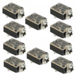
Also the audio connector is wrong in that order.
The guy who put the PCB board together decided to go with a really strange stereo audio which has 5 pin(!) connection to the PCB. Not that common to find vs a 3 pin version.

I finally sourced the type I needed from eBay
s-l1600.jpg

Take a look at the top of the unit and it will have a weird spring based design inside with a transparent top

UTSource also failed me on finding a TEA2025 amplifier chip. They contacted me to say they could not find any TEA2025 16DIP only surface mount ones!

I cancelled that part but I am still waiting for them to send me:
74LS245
SAA1099 x 2

I went on eBay and purchased the requried TEA2025 16 DIP instead

Getting all the parts for this project is some what of a challenge as many of them simply don't want to sell DIP chips only the surface mount versions, something that will get increasingly difficult as time goes by
 
Hello guys. First time poster here. I recently found out about this cool do-it-yourself project and built one myself:


In terms of components I bought all parts (well almost) from Digi-Key. The Philips SA1099P and TEA2025B I bought on Ebay. I went with a trimmer style 10K Ohm for the potentiometers. They are small enough not to block the expansion slot next to it. I left them at a desired value and use my speakers to control volume.

When I first installed the card the music sounded distorted. Like somebody else mentioned earlier on this thread the volume level on the card was amplified way too high. The microchips I bought were not plain original versions but revisions with a letter next to them (eg, SA1099 with a "P" suffix, TEA2025B, 74LS245N, etc.) I am not an expert and thought maybe this was to blame. After lowering the pots down to about 0.35 (very low!) the card sounded like I used to remember from way back then. Other than that hiccup everything went fine. Maybe a future revision might address this.

Thanks veovis for sharing your project on github. I've yet to drill a hole on the computer bracket but so far this has been a fun project!
 
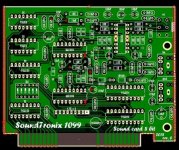
I have nothing to do with the SoundTronix cards and I could find very little about them with a quick search. The PCB layout is completely different so I suspect this is the result of some else's attempt to recreate the Game Blaster and perhaps add one or two features (I see a line out for one thing.) At least I hope that is what this is.

If this was originally based on my schematics then this design should be published as open source as well. However this design does appear to be significantly different than mine so I am inclined to believe that this may be the result of a completely independent design attempt.
 
I'm working on the audio chipset for the Commander X16 machine, and built a small SAA1099 test board for the X16. While it is working, the audio was noisy. I then looked at the schematic for the Snark Barker as I suspected Creative had designed a good circuit for this already, and I then thought, hey, I'll build an ISA Gameblaster clone! This would give me a way to tweak the audio and get it right for the final X16. I never even bothered to look around on the internet or even the Gameblaster itself, I just thought I already built this on the X16, so no biggie for ISA! So, it does work, but for some reason I decided to look at the actual Gameblaster card while I was assembling my prototype. I saw the honking chip on it, panicked, then spent about 2 hours reading and found Sergey's detection circuit.

So no problem to fix, but I had a question before I made another version. I did look at the Snark Barker for another reason however, and that is the IOR line handling. I also noticed that no one else seems to be implementing it. I used a 74ACT125 as a trigger on this line, but now I'm wondering, do I even need it? I also wonder if there would be a huge benefit to using the IRQ line on a card like the original Adlib. Interestingly, it had the IRQ plumbed, but not soldered. I'm sure the code for most sound chips is just timed to allow the sound chip to be ready before the next write. Likewise, I suspect no one was really using the IOR line on the ISA bus even though it IS connected on the SB Pro 1.0 and I suspect the original Gameblaster? It certainly sounds like everyone's clones are working, but has anyone run into code out there that checks IOR? If some games are failing, this may be why. IOR is a bit scary, and I may have this description wrong, but I thought the idea was to invoke this line when a write to the device "fails" because it is busy. This way, I could probe and know if the write was successful or not. However, IOR halts the bus as I recall, and if you do it for too long, it can hang the system. Just talking from memory, but even if I'm a little off on this description, I do know messing with this line can crash a PC. :)

Thanks!
Kevin
https://texelec.com
 
Kevin, The /IOR and /IOW signals (pins B13 and B14) most certainly are used on the Gameblaster and are required for most ISA cards to function since they are the signals that determine whether a particular address is being read or written to so I am confused about what exactly you are talking about.

Could you be talking about pin A10 (IO CH RDY)? If so, as far as I am aware the sole purpose of that pin is to allow ISA cards to temporary halt the ISA bus to allow more time to process a memory access request. It is very rarely used and I don't think I have ever seen a sound card use that line. It is certainly not something software most software can use or even check for and in general halting the ISA bus is a bad idea unless you have a very good reason for doing so.
 
I am talking about IO Ready, sorry, that was ambiguous. And yes, the GameBlaster, as well as the SN76489 on the PCjr both use it in the way I describe. Yes, it is scary, but the Snark Barker/SB 1.0 both use it.

See the schematic: https://github.com/schlae/snark-barker/blob/master/SnarkBarker.pdf

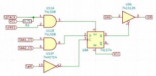
Ahh, the IO Ready signal! I'm dealing with a similar signal right now on the MCA Ad Lib design. So here's why you need it:

From the SAA1099 datasheet, page 10:
In most bus cycles DTACK# will be returned immediately, this applies to all register address load cycles and all except amplitude data load cycles. With respect to amplitude data, a number of wait cycles may need to be performed, depending on the time since the previous amplitude load. DTACK# will indicate the number of required waits.

The SAA1099 occasionally needs the data to be held on its data inputs for multiple cycles of the 7.159MHz input clock. Normally when you write to the part it will immediately pulse DTACK# but in the wait state case, it may take a few additional cycles before the DTACK# line pulses.

In the Sound Blaster/Snark Barker, there's a latch, U20B, that controls the ISA bus IO Ready signal. When either SAA1099 chip is selected (CS# goes low) and WR# pulses low, the latch clears, driving a '0' through the 74LS125 buffer to IO Ready. The latch remains in this state until either SAA1099 chip asserts DTACK# or the ISA bus reset signal asserts. When that happens, the latch returns to the set state, driving a '1' to the 74LS125 buffer which then releases IO Ready. Technically you can also clear the latch by writing to some other address (SAA1099 CS# lines are high) but this probably depends on the specific ISA bus motherboard design.

The 74LS125 is just used to produce an open drain output since IO Ready is shared with all the slots on the ISA bus. You could easily replace it with a transistor or an open drain logic gate.

If you leave out this circuit, the SAA1099 may run into issues where it will not properly latch amplitude data.
 
Thanks so much! I had read that before, and your explanation definitely helps. I guess it just pulses once when the write is done? I'm not sure how to hook this event in code, will have to read a bit... This seems an odd way to handle what is essentially an interrupt, but I guess it is just another method to accomplish the same thing.

A lot of the clones may be missing a small bit of the circuit which is at times, critical. Since this circuit was on the original HW, I can only assume that at least sometimes, the code was not "timed" to avoid this problem. I think I will add a jumper to make this line optional though in case someone wants this disabled for some reason. As it turns out, I pretty much copied the Snark Barker design. I had fumbled around with this on the SN76489 a few years back, and have always been terrified about feeling confident about a circuit design. This is why I like what the SB did, it makes sense and seems a lot cleaner than just tying the Ready line(76489) straight to IO Ready like the PCjr! I mean it is IBM and imagine they tested it, but I think there were hangs associated and I suspect this circuit would have been revised later if the PCjr had stuck around longer.

At the risk of digressing too much, on the Commander X16, I don't really have a IO Ready line to speak of, and I've just been thinking of ignoring it there and making sure the folks know they need to delay a certain amount of time to allow certain writes. We will likely have a BASIC routine if we wind up using this chip to play notes which means you won't even have to think about it until you are in ASM or C, and its just something we need to document well. It will take some testing, but it seems like this chip is simple enough to be able to predict the number of cycles needed in each case. I do like the idea of a latch with a separate memory address. This would fit nicely in the 6502 world, but I'm trying not to add too many more parts.

ioready.jpg

Thanks again for your help!
 
Last edited:
Got one of this kits from ebay:

Seems very similar to this one but no identical, is the same project ?.


https://www.ebay.com/itm/PCB-SOUNDT...e=STRK:MEBIDX:IT&_trksid=p2057872.m2749.l2649

Hi friends, I am glad to see this wonderful whiteboard to draw with me. I can say that there are two errors in this board, and I can also say that this is a Tronix invention, which means that MUS was borrowed from the Tronix circuit. Personally, I changed the decoder in this board, built according to the MUS scheme.
 
Now I changed the board, removed the errors and installed 7805, this board will be on sale soon.

1троникс.jpg
 
Back
Top