• Please review our updated Terms and Rules here

Disabling DOS/Deskmate-in-ROM on a Tandy 1000 HX: Close! But... ideas?

Eudimorphodon

Veteran Member
Joined
May 9, 2011
Messages
7,074
Location
Upper Triassic
As the thread title indicates, lately I've been fooling with an idea for increasing the amount of upper memory space available in a Tandy 1000 HX. To recap, the major internal difference between the HX and the otherwise similar EX is the HX has a whopping 128K of BIOS ROM, which according to various sources and spelunking on my own is set up like so:

E0000-EFFFF: Personal Deskmate resources (64k)
F0000-F001F: Simple ROM-DOS BIOS option ROM. (.5k)
F0020-FBFFF: Minimal DOS 2.11 FAT filesystem (47.5k)
FC000-FFFFF: Phoenix/Tandy PC BIOS. (16k)

The EX only has the 16k BIOS, although because of incomplete memory decoding all 64k of the F-page is still effectively off-limits. However, the "E" page is available for UMBs, EMS page frames, whatever.

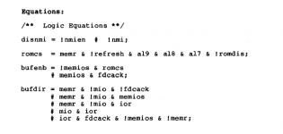
Anyway: while looking through the HX's tech manual I found that the ROM is decoded by a PAL at position "U16", and the equations are in the manual:
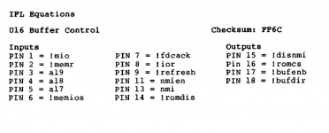
PAL-PINS.png
PAL-EQUATIONS.png

According to the equations ROM enabled when A19, A18 and A17 are high (IE, CPU in the top 128k of the memory map) unless pin 14, labeled ROMDIS, is pulled low. Checking the schematic indicated that ROMDIS is just permanently tied to a pull-up resistor, R21A:
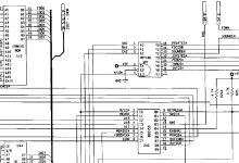
schematic_frag.png

So... I attached a test clip to the U16 side of R21A and checked with the logic probe to see if the state on that pin was ever anything but high; it wasn't, so I proceeded with experimenting with my homemade memory board that can map upper memory blocks and an EMS page frames using GALs as decoders.

To try to make an already long story as short as possible: first I tried putting upper memory and/or an EMS page frame in the "E" page by simply configuring the switches on my memory board to think it was in an EX instead of an HX and connecting the jumper wire to U16 pin 14 to pin 19 on the 74HCT245 that sits in front of all the memory devices on my board; that seemed like it should work, since it would effectively let the expansion board trump ROM if anything on it clashed. And that worked, just fine. Dropping the EMS frame into E0000-EFFFF and testing with Checkit confirmed no conflict.

(And, for the record, when just the E-page is overridden the DOS-in-ROM is still there and can be booted, it has no apparent dependency on the E-page contents. Presumably the HX version of Personal Deskmate won't work, but I didn't try it.)

Here's where things get weird: Since the DOS-in-ROM "driver" presents itself as a normal BIOS extension my next test was to reprogram the GAL on my memory board to try replacing the built-in DOS with the XTIDE BIOS stored on a flash chip on the card. That didn't work; the DOS ROM *is* overridden, but peek-ing around at the F0000 mark shows garbage that's neither the built-in ROM nor the XTIDE BIOS. Here's the weird part, though: this "garbage" is only present from F000-F1FFF; I had the GAL configured to override 32k, and after the F2000 mark PEEK-ing shows nothing but zeros, which is expected; the ROM is blank except for the first 8k.

After several iterations of being sure I must have made a mistake in my GAL programming for the ROM mapping I decided to remove the dependency on the memory buffer and set up a spare I/O pin as independent signal that would effectively disable all but the last 16k of the built-in ROM, no matter how things were otherwise set up on the board. This works as expected, the ROM DOS is gone, but things are still weird over the F000 mark. Here's what I see when I peek around that area:

1: From E0000-EFFFF if I don't map anything there the area is full of "7",s; this is what you see on this machine if you peek in an unoccupied area of upper memory, so the "ROMDIS" line seems to be completely doing the needful.

2: From F0000-FBFFF there's "garbage" that's mostly decimal 240, with the occasional 176. The "176s" are different from run to run, like the data lines are just floating.

Whether I piggybank off the buffer signal or go with the separate line pulling down ROMDIS the results are still the same if I try putting my ROM at F0000; I get garbage. I haven't yet tried dumping it to see if it has some bitwise relationship with the ROM contents, but... I'm kind of at a loss. Does anyone have any idea why the HX treats the F-page differently from the E-page if the ROM is disabled? (And, even more specifically, why it seems to be treating the 8k from F0000 to F2000 even more strangely, since it seems like the ROM override is working okay from F2000 to F8000?) I'd suspect that the PAL equation was incomplete, but there's no connection from the PAL to A16 so far as I can tell it can't tell the difference between E and F. Staring at the schematics haven't given me any "aha!" moments.
 
Last edited:
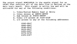
Maybe answering my own question? In the specifications document for the Big Blue video processor used in the EX/SX/HX/TX I found this:

BigBlueF000.png

The signal in mentions there, ROMIOSELB, doesn't actually appear on the chip package; I'm guessing Tandy couldn't decide what it was called because a couple pages later where the pinout is described there is a signal on pin 31 called "IOMEMSELB", described as "External Buffer Disable", which seems to be what "ROMIOSELB" is actually referring to. The HX schematic calls pin 31 yet another name, "MEMIOSEB", on the schematic signal, and that's what's connected to the "!MEMIOS" line, pin 6, on the PAL.

Anyway, the salient point seems to be that the Big Blue itself is hard set to think ROM fills all of the F page, so it will try turning on the '245 buffer in front of all the motherboard devices when the address is in that range regardless of what the "accessory" decoder for the 128K ROM does. If this is what's happening then it explains why my ROM on the address bus gets trashed even if I pull "ROMDIS"; the bus is still going to get whatever random noise there is north of the motherboard buffer pushed onto it by said buffer because Big Blue is asking for it.

The only thing about that theory that, well, maybe I'm thick today. The PAL equation says this:

PIN 6 = !memios
PIN7 = !fdcack
PIN16 = !romcs
pin17 = !bufenb

buffenb = !memios & romcs
# memios & fcdack

If I write this in english, compensating for the inversions, I think this means:

if memios = 1 and romcs = 0 then buffenb = 0 OR
if memios = 0 and fdcack = 0 then buffenb = 0

I don't think that second one can be true and there must be a typo, because according to the schematic "fdcack" is a DMA-related line that in an HX without a DMA chip is tied to a pull-up resistor. Therefore fdcack would always = 1, and if it always equaled one then no I/O or memory read/write transactions to the Big Blue chip would *ever* succeed. The logic therefore *has* to be:

if memios = 0 and fdcack = 1 then buffenb = 0

I guess I should stick a probe on it to be sure.
 
So... apparently the forum isn't letting me attach any more pictures to show it off, but I'm now successfully booting a Tandy 1000 HX motherboard from an XTIDE BIOS sitting on the expansion bus at F0000.

Per my previous post, I was right about the !fdcack line; if I pull it down with the same dedicated override signal I'm pulling !romdis down with all traces of the built-in DOS ROM go away, along with the junk-ing of an accessory ROM mapped at F000.

Just jumpering to both of these pins is not a perfect solution. The FDCDACK line in question here terminates three places:

1: Pin 7 on U16
2: B26 on the bus connector
3: Pin 15 on the PD765 FDC chip.

On the FDC chip /DACK is described as "DMA Acknowledge: When the DAC input is low, a DMA cycle is active and the controller is forming a DMA transfer". I know the Tandy ties this to the expansion bus so if an accessory DMA controller present it'll let the built-in controller use it. I guess the question I have is: is it likely to cause problems if this input is asserted on the chip at random times due to memory accesses? I assume it won't, because the chip will have been set up to do polling I/O, but... ? Floppy I/O seems to be working fine with this setup, but is it possible there could be some weird edge case where an access to upper memory overridden this way causes some sort of screw up?

A cleaner thing to do would probably be to program a new 16v8 to replace the original PAL so pulling ROMDIS also overrides the memios line; then I only need one jumper to fix everything. Unfortunately I also know now that the equations for this PAL have to be wrong. Does anyone know if the actual contents of an 82S153 can be read out in a cheap modern programmer like an TL866 and converted back into an equation, or is this PAL likely to have a security fuse or other complications?
 
Regarding the PAL programming, I've compared the manual for the HX with the EX and SX, and I think I'm convinced that similar typos were propagated through all three. The EX says:

Equations:
/** Logic Equations
bbrfsh = refresh;

!bufdir = memr & !mio & !fdcack
# imemr & !mio & memios
#memr & !mio & ior
#ior & mio
#ior & fdcack & Imemios &Imemr;

!bufenb = !memios & !romcs & !fdcack
#imemios & fdcack;

romcs = memr & !refresh & al9 & al8 & al7 & al6;

iomb = mio;

enbnmi = nmien & nmi;

The "bufenb" equation is identical in the SX. Interestingly the pin list still shows "bufenb" with a "!" in front of it, so essentially there's a double negative in the EX/SX manuals. If I believe the double negative is intentional, which I'm not sure it is, I think it translates to:

Code:
Buffer is enabled if:

MEMIOS is YES; ROMCS is YES; FDCACK is YES

OR

MEMIOS is NO; FDCACK is NO

This makes no sense because the only conditions under which the motherboard buffer would be open is if anything *but* the IO/memory on the big blue or ROM was being accessed OR an FDC DMA request was being acked. If I remove the double negative and make it just a single negation for bufenb then I get:

Code:
Buffer *is* enabled if:

MEMIOS is NO; ROMCS is NO; FDCACK is NO

OR

MEMIOS is YES; FDCACK is YES

This still makes no sense because we still end up essentially never able to reach the big blue *unless* an FDC ack is happening at the same time. If, however, we get rid of the both the double negative and input negation on fdack it's:

Code:
Buffer *is* enabled if:

MEMIOS is NO; ROMCS is NO; FDCACK is YES

OR

MEMIOS is YES; FDCACK is NO

Now the buffer is open if an FDC ack is being handled by something outside of the ROM or big blue memory *or* Big Blue, F0000-FFFFF, or the associated I/O ports on the motherboard are being accessed and an FDC ack is *not* being handled. This seems like the closest to reality?

Alternatively, if I don't get rid of the double negative but get rid of FDACK's negation:

Code:
Buffer is enabled if:

MEMIOS is YES; ROMCS is YES; FDCACK is NO

OR

MEMIOS is NO; FDCACK YES

This means Big Blue I/O will only be available if ROMCS is also true, so, no, this doesn't work. So by process of elimination I'm voting that both the EX and SX manuals have a faulty double negative on the buffer I/O pin state, and have a faulty single negation of FDCACK. So, now, going back to the HX equation, if I get rid of the negation on FDCACK its equation of:

bufenb = !memios & romcs
# memios & ! fdcack;

Would translate to:

Code:
Buffer is enabled if:

MEMIOS is NO; ROMCS is YES

OR

MEMIOS is YES; FDCACK NO

Which is "Enable the buffer if the ROM is selected or if big blue I/O or memory is active unless an FDC DMA request is being acked." I'm willing to buy that as true.

So, whee. At this point if I had any GAL16v8s I'd try programming one and seeing if that one change fixes it. But I don't have any, so... next Digikey order, I guess.
 
Aaand, responding to myself again:

On the FDC chip /DACK is described as "DMA Acknowledge: When the DAC input is low, a DMA cycle is active and the controller is forming a DMA transfer". I know the Tandy ties this to the expansion bus so if an accessory DMA controller present it'll let the built-in controller use it. I guess the question I have is: is it likely to cause problems if this input is asserted on the chip at random times due to memory accesses? I assume it won't, because the chip will have been set up to do polling I/O, but... ? Floppy I/O seems to be working fine with this setup, but is it possible there could be some weird edge case where an access to upper memory overridden this way causes some sort of screw up?

I read through the 765 FDC datasheet, and it looks like until I can replace the PAL I'm probably safe driving both ROMDIS and FDCACK low to override the Fxxx section of ROM with my memory board because the FDC chip shouldn't be programmed to use DMA mode in my computer, since I don't have the original DMA plus card. Also I don't think there's any way the combination of signals that would cause the FDC to think that a DMA read or write cycle is being performed could actually be triggered without said DMA controller even if the FDC were misprogrammed to try to do DMA: the necessary condition would be the address bus would have to be somewhere in the affected upper memory region at the same time the IOR or IOW signals are asserted. I don't think that's possible; if the CPU, not the DMA controller, causes IOW/IOR to be asserted I *think* the upper address bits will be automatically be zeros, which removes the possibility of accidentally having FDCACK asserted alongside IOW/IOR.(*)

(* I'm sure someone smarter than I about low-level 8088 goo could correct me on this.)

If the DMA controller *were* present then this still might "work", but pulling down FDCACK would require fighting the DMA controller unless it uses an open collector to pull down FDCACK? So, probably not recommended.

An interesting thing about this whole deal: in theory at least I should be able to replace *all* the ROM, including the BIOS, with flash on the expansion connector if I want to. I wonder if it'd be possible to reverse engineer enough of the differences between the HX and TX BIOSes to make the EX/SX/HX capable of taking 640k of expansion memory and behaving like a 768k TX with regard to video...
 
Last edited:
Very nice so you are developing a memory expansion board for the tandy 1000 HX ?, to get 1024k of ram or EMS ?.

My latest version has a total of 1.5MB; 384k to backfill it up to 640k, 128k that can be mapped in upper memory for loading dos/drivers high, and 1024k of EMS. (Most I could fit on the board with through-hole memory chips; I need to learn to solder surface mount; if I did that I might be able to stuff as much as 4.5MB without changing the architecture.) Also has two serial ports, an XT-CF storage system, and the standard Plus expansion passthroughs.
 
Just so no one can say "pics or it didn't happen", here's a couple screenshots:

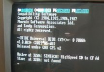
XTIDE BIOS initializing at F000:

XTIDEatF000.jpg

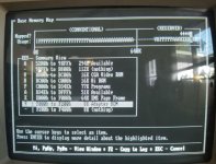
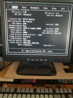
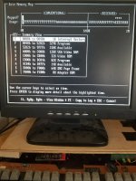
And here's a Checkit3 memory map showing 128k of upper memory from C000 to DFFF, an EMS page frame at E0000-EFFF, and an 8k "Adapter ROM" at F000. (Note that main RAM stops at 9BFFF, as expected in a Tandy 1000.)

128kUMBs.jpg

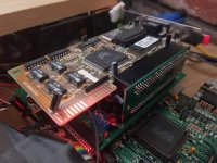
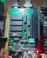
Here's a not particularly enlightening picture of my test setup as I've cleaned it up for now. The gray wire coming off pin 19 of the GAL 20v8 in the upper right of the board is the source of an override signal that kicks in from E0000-F7FFF. You can't really see it clearly because it's obscured by my ISA riser board, but one end of a black jumper clip wire is connected to B26 on the left expansion bus header; I'm using that to grab the FDCACK signal because it's easy and accessible. The other end of the jumper wire is clipped on the PAL side of resistor R21A and the other end of that override wire.

expansionhack.jpg

It's working, but I'm sure the clip connector might be prone to glitching so this setup is by no means permanent. If I can figure out the equations to program a suitable replacement for the PAL I'll be able to eliminate the FDCACK wire and get it down to a single jumper, which should also make this compatible with HXes that have the Tandy RAM board with the DMA chip.

(The E000 override should work fine in a DMA-equipped HX, it's the F000 page that opens up the can of worms.)
 
Now... witness the power of this FULLY ARMED AND OPERATIONAL BATTLE STATION!

So, in the slight chance anyone was playing along and hadn't guessed, this is where my interest in freeing up the wasted UMB space on my Tandy 1000 HX-based hackputer came from. Behold the stack of ridiculousness:

cardstack.jpg

That's an OAK OTI-077 VGA card on top, under it is a Realtek 8019A network card. Only been testing for an hour or so, but so far both work.

checkit_conf.jpg

Checkit shows VGA, also shows the 16k normally reserved in a Tandy 1000 now counts as system memory for 640k base.

checkit_memmap.jpg

Checkit memory map. The address space is now officially full.

(The default configuration of my memory card when set for an HX normally puts the XUB at C000, makes everything otherwise unused up to DFFF upper memory blocks, and puts the EMS page at A000. Neither C000 or A000 is an option with a VGA card plugged in, making the choices effectively: 1: no upper memory blocks 2: no EMS, or 3: hack it, and hack it hard.)

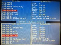
Topbench_VGA.jpg

Topbench says the VGA card is microscopically faster than the built-in video memory, but it could just be sunspots tweaking the needle.

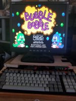
bubblebobble.jpg

And, yes, it will run EGA Bubble Bobble with Tandy sound.

This whole affair of sticking in a VGA card of course badly and hypocritically violates my standard argument that the main reason to have a Tandy 1000 is for its unique video system. And I still mostly think that. But, hey, if a mountain is there you need to climb it, right?
 
Very cool and you got a lot of free ram there :D.

I've made it even a little bit crazier; per this thread I've written a little "enabler" that lets me use the EMS page frame as an additional 64K of UMBs just in case there's some situation where maximum base RAM with a ton of drivers installed is more useful than EMS. I'm going to try testing that out with an NFS file sharing stack ASAP. (Said stack takes almost 60k of RAM.)

Practically speaking why anyone needs all this in an HX, well... "because you can" is clearly the only valid answer. :)
 
Last edited:
Having some extra UMBs space in the tandy HX and SL is something very handy indeed for tandy owners.
Hope your project get to "mass production".

Do you use or plan to use only dip packages or you will use smds ?.
 
Having some extra UMBs space in the tandy HX and SL is something very handy indeed for tandy owners.
Hope your project get to "mass production".

I don't have an SL, alas, but I do wonder if a similar technique would be possible to override its ROM DOS. I have this feeling it might be somewhat less trivial, unfortunately. With the 8086 there are bus size issues, and I assume the ROM is 16 bits wide in those machines? (I honestly don't know off the top of my head.)

What I really need to do is sign up someone to help me figure out if it's possible to kitbash the TX BIOS so the "768k mode" can be backported to the EX/HX/SX. Since installing the VGA card I've been running some benchmark programs to satisfy my curiosity about how the "Big Blue" RAM performs when it's not doing video refresh, and the long and short of it is these machines take a pretty large performance hit whether you have a VGA card installed or not because that part of RAM that's backfilled with video memory runs at an effective 4.77mhz-ish thanks to wait states. If we could override the ROMs in the EX/HX/SX with a hacked version that would test for expansion memory up to 640k and switch Big Blue to the "Video Only" mode like the TX then it would be a significant speed boost for large memory applications. (I have confirmed with manual experimentation that the EX/HX support the necessary mode, just need the BIOS support for it.)

Granted whether it'd be worth anyone's time is a totally valid question. ;)

Do you use or plan to use only dip packages or you will use smds ?.

My board is all through hole:

expansionhack.jpg

I've been thinking of trying to do one with surface-mount RAM chips, since 3x512k is the maximum that's feasible in the space available with all the other features on the board; they make a suitable 2MB RAM chip and in theory the EMS page registers layout can support up to 4MB. Of course I haven't really come up with a good use for the 1MB I have.
 
Back
Top