jmdhuse
Experienced Member
Hello All,
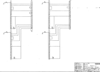
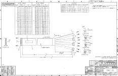
I am on a mission to track down the details of this ECO, which, as I understand it, is applied to an etch rev D to correct an IO register addressing anomaly. The information I have regarding this problem and ECO is from one of the micronote documents, which is quoted below.
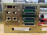
I have both an etch rev D module (5013216D-P1) and etch rev E module (5013216E-P1), and I am determined to track down the details of the ECO.
Here is what I have done so far:
Using the MP-00586 schematics, I have modeled the decoding logic with a small C program and verified that the proper addresses are decoded. I have ohm'd out the decode logic of the rev D board, comparing it to the schematic, and haven't found any disagreement. This is confusing, because it suggests the schematic is the same as etch rev D, but there is not problem seen.
What I'd like help with is this: Does anyone have a rev D board that shows evidence of the ECO, which is indicated by the presence of a green ECO wire. If you have such a board, could you post a picture of the ECO wiring, so I have some idea of what the ECO is actually doing.
I know this is not a vital investigation, but what else are hobbies for? I'd like to be able to provide the information for anyone to modify their rev D board so they behave like the corrected rev E boards.
Thanks, Jon.
Here is the entry from the micronotes document regarding this problem and ECO:
DLV11-J I/O Page Address Problem Report
PROBLEM
Under certain conditions, the DLV11-J will falsely respond to bus cycles intended for other bus interface modules. When this happens, the DLV11-J address selection logic will be enabled, in addition to the address selection logic of the correct module. This results in the DLV11-J placing information onto the bus which will be OR'ed with the data from the correct module.
NOTE: DLV11-J modules at Circuit Schematic (CS) Revision E or above do not have this problem.
CONDITIONS
1) This problem will occur only when the program is performing a bus cycle that accesses the I/O page and will not occur for accesses in the 0-28Kword address space for the LSI-11.
2) This problem will occur only on DLV11-J modules that are configured to have a console port.
3) This problem is more noticeable with the 11/23 and with DMA transfers on the LSI-11 and LSI-11/2.
PROBLEMS OBSERVED
1) This problem has been noted to occur when using the bootstrap in the REV11 module to load paper tape. In this case, the REV11 ROM command "AL177560" will cause an abort to ODT. However, the command ''AL CR" will work properly.
2) Program failures and data errors may be noted when using the 28K to 30K area in the I/O page for program memory.
3) Errors may also be noted while using other I/O interfaces which have certain address bits (notably bits 5 and 8-12) that are similar to those used by the DLV11-J.
SOLUTION
Install ECO M8043-002 on the DLV11-J. This ECO brings the CS up to Revision E.
All modules processed by the Customer Repair Area (CRA) will be updated to this ECO. This update will be performed at no charge to the customer. This customer should obtain a no-charge SBA from his Sales Specialist in order to have the module updated.
QUICK CHECK
The presence of green wires or of CS Revision E or higher indicates that this ECO has been installed.
NOTE: This ECO IS REQUIRED FOR ALL DLVI1-J MODULES USED WITH THE LS1-11/23.


