Another thought to see if the DMAC is having problems driving the address lines, you could use the /BGACK signal as the trigger instead of /AS. It would be better to be able to trigger on both /AS and /BGACK low, but if you only have a two channel scope, that is hard unless you were to use a supplementary logic gate to or them together.
| VCF West | Aug 01 - 02 2025, | CHM, Mountain View, CA |
| VCF Midwest | Sep 13 - 14 2025, | Schaumburg, IL |
| VCF Montreal | Jan 24 - 25, 2026, | RMC Saint Jean, Montreal, Canada |
| VCF SoCal | Feb 14 - 15, 2026, | Hotel Fera, Orange CA |
| VCF Southwest | May 29 - 31, 2026, | Westin Dallas Fort Worth Airport |
| VCF Southeast | June, 2026 | Atlanta, GA |
-
Please review our updated Terms and Rules here
You are using an out of date browser. It may not display this or other websites correctly.
You should upgrade or use an alternative browser.
You should upgrade or use an alternative browser.
Ensoniq EPS classic repair. 68k cpu
- Thread starter foofles
- Start date
Yes, yellow is address and pink is AS. A1 is labeled if you mouse over the images. It's the 3rd one for some reason.
I changed to falling edge trigger, thanks.
There's nothing in the expansion connectors when I'm testing things.
I do have a desoldering station. It was just a bit clogged when removing the last chips which lead to a bit of damage... Trust me, I've looked low and high for solder bridges. Given that it gave error 18 before and after all the work I've done on it, I think there's def something other than a solder bridge from my work (though I def could've made one that'll need fixing)
-----------------------------------------------------------------------------------------
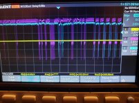
I took some better pictures after my last post. All of the address lines that I'm looking at do go low and high at points when AS is low. I have not seen iffy looking address signals when AS is low. So I guess address lines are okay?
All pull up resistors I've tested have been good.
I couldn't find every pull up resistor that I wanted, so I measured resistance from pins to ground and 5v. They all got the proper 3.3k resistance to 5v.
However the resistance between ground and 5v was only like 350 ohms ....
BGACK is never low. The DMAC never asks to take control of the bus from what I can see. It never moves even on bootup.
"However, the ~0.4 V shifts on the A1 line could be indicative of a problem. It looks like the A1 line isn't reaching the low level correctly, but you might try a few more captures on A1 and A2 to see if you can see they are being driven to both the low and high levels when /AS is low." I assume you mean that first image I posted. I think that was A3. I can test them all again, but they were going high and low when AS was low.
And regarding printing it - yeah, I had to get a print shop to print it off on a giant sheet of paper for me. Helps a ton!
I changed to falling edge trigger, thanks.
There's nothing in the expansion connectors when I'm testing things.
I do have a desoldering station. It was just a bit clogged when removing the last chips which lead to a bit of damage...
Trust me, I've looked low and high for solder bridges. Given that it gave error 18 before and after all the work I've done on it, I think there's def something other than a solder bridge from my work (though I def could've made one that'll need fixing)-----------------------------------------------------------------------------------------
I took some better pictures after my last post. All of the address lines that I'm looking at do go low and high at points when AS is low. I have not seen iffy looking address signals when AS is low. So I guess address lines are okay?
All pull up resistors I've tested have been good.
I couldn't find every pull up resistor that I wanted, so I measured resistance from pins to ground and 5v. They all got the proper 3.3k resistance to 5v.
However the resistance between ground and 5v was only like 350 ohms ....
BGACK is never low. The DMAC never asks to take control of the bus from what I can see. It never moves even on bootup.
"However, the ~0.4 V shifts on the A1 line could be indicative of a problem. It looks like the A1 line isn't reaching the low level correctly, but you might try a few more captures on A1 and A2 to see if you can see they are being driven to both the low and high levels when /AS is low." I assume you mean that first image I posted. I think that was A3. I can test them all again, but they were going high and low when AS was low.
And regarding printing it - yeah, I had to get a print shop to print it off on a giant sheet of paper for me. Helps a ton!
Just a quick rundown of the current behavior - it starts, loads the OS from the floppy, then after a very short moment gives error 18. It sits at an "insert disk" message if a floppy is not inserted. It reacts to button presses to restart on the error 18 screen. So some stuff is working.
The document I was just reading mentioned that error 18 could be a bad DOC II chip (the custom IC that makes the sound!)... which would be bad since I can't get a replacement.
I'm going to do more investigating on the DOC II tonight.
The document I was just reading mentioned that error 18 could be a bad DOC II chip (the custom IC that makes the sound!)... which would be bad since I can't get a replacement.
I'm going to do more investigating on the DOC II tonight.
Ok, sounds like the address lines are ok if it boots at all. Too bad if it were the DOC II chip, perhaps you can find a donor unit for that.
As for the resistance between +5 and ground, that is probably ok, there will be a lot of capacitors to charge and after that happens then there will be various pull up resistors and other components that will draw current.
As for the resistance between +5 and ground, that is probably ok, there will be a lot of capacitors to charge and after that happens then there will be various pull up resistors and other components that will draw current.
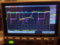
How concerned should I be about the voltage levels not quite hitting 5v for some things and going negative for some things... See image. Taken last night, not sure which signals exactly these were... Glue logic for the ram, I think. Regardless, they're going almost to -5v here! What could cause this?
Yellow line is at 0v.
Yellow line is at 0v.
Attachments
What is the bandwidth limit of your scope set to for each channel? Not reaching 5V or all the way to 0V on logic lines is common, especially with the older TTL logic families, as long as the high and low levels are well beyond the logic family's thresholds. CMOS chips do a better job usually of getting closer to the rails, unless heavily loaded by inputs.
Since there is no negative logic voltage in use, you might also check that there is no short from the analog -VA rail to something else. Of course it would be helpful to know where you were probing when you grabbed that snapshot.
Since there is no negative logic voltage in use, you might also check that there is no short from the analog -VA rail to something else. Of course it would be helpful to know where you were probing when you grabbed that snapshot.
It's a 100MHz scope. The negative spikes don't disappear. They aren't *quite* as bad with shorter leads, but they're still there.
I found something interesting though. Looks like a bad 74ls244 to me. It normally works as expected, but then suddenly I'll see /E low with Y1 not matching A1. Pic attached of one of these incidents. Y1 was moving at other times. I'm about to go try to recreate it again.
I found something interesting though. Looks like a bad 74ls244 to me. It normally works as expected, but then suddenly I'll see /E low with Y1 not matching A1. Pic attached of one of these incidents. Y1 was moving at other times. I'm about to go try to recreate it again.
Attachments
Ok, since you have an error code that has to do with the DOC II chip, concentrate on the signals going to/from it. I just downloaded the datasheet for it, it will take me some time to read it and figure out what it does with its pins. It is clear that it manages the DRAM access, as well as responds to the CPU's access to the DOC II's internal registers.
Start with this: check to see when /DOC (bus name) aka /CS (chip name) signal is asserted (low) at pin 6, that /DTACK is asserted (low) in response on pin 4 a cycle or so later, which presumably accesses the I/O registers in the chip.
Start with this: check to see when /DOC (bus name) aka /CS (chip name) signal is asserted (low) at pin 6, that /DTACK is asserted (low) in response on pin 4 a cycle or so later, which presumably accesses the I/O registers in the chip.
Also make sure you have a copy of the EPS Technical Manual https://drive.google.com/open?id=1v7JlYQHTrD3Hf7Tw7OLxh1jksgm066g2, which looks like is describing how the synth is designed to work.
What version of the ROMs are installed in your unit? Perhaps a disassembly to see what triggers error code 18 will be useful.
That's what I had been working on, actually. Not sure what version I have on my unit - I dont have anything handy to dump the eproms. Technically I could rig something up with a microcontroller and shift registers or something though.... I probably need to wire up some shift registers to drive the 14 address lines of the system ram to test it too.
The eprom dumps are on that site somewhere - it's in a high and a low byte file. I wrote some code to combine em into a single file, but I can't seem to get a disassembler to work on it. I have never used a disassembler though. I can see various error messages and other text messages in the combined file, so I assume I didnt screw something up combining them.
Any pointers on disassembling? I tried running it through ghidra but had issues.... will edit this in a bit with the exact error it gave. Edit - "/* WARNING: Control flow encountered bad instruction data */". I'll try to read up on how to operate ghidra unless you know of a better solution for 68k dissassembly
And please don't waste much of your time looking at the technical manual or the doc II datasheet! There's pretty good info in em though.
"Start with this: check to see when /DOC (bus name) aka /CS (chip name) signal is asserted (low) at pin 6, that /DTACK is asserted (low) in response on pin 4 a cycle or so later, which presumably accesses the I/O registers in the chip."
I will look at this and anything else I can think of on the doc II chip soon!
Last edited:
I was going to suggest ghidra as a possibility for the disassembly. The 68000 reset vector is a the start of the ROM image, so assuming you have the byte order correct it should be able to start finding some stuff. It may be possible that error 18 is generated by the OS code which gets loaded off the floppy. The DOC II is responsible for managing the dynamic sound RAM (labeled SRAM in the tech manual - which is not the static ram which is labeled OSRAM) addressing and refresh, so it may also be possible that if there is an issue with the dynamic RAM the DOC II could be blamed in the error code. But start with seeing if you can figure out if it is responding to register accesses by the CPU. A logic analyzer would be very helpful at this point.
Actually, I forgot that the first thing the CPU will read from the start of the ROM is the reset vector, not code. So you'll have to use the first four bytes as the address of the reset code in the ROM. It is likely that this will lie within the decoded address space for the ROM, so you will need to tell ghidra what the base address of the ROM to get sensible results.
I've replaced all glue logic related to the dram and tested all of the dram chips. U13, which I believe is what the cpu uses to send a 4 bit address to the doc in order to read register values,has a brief spurt of activity at the moment it gives error 18, so I've been thinking that the cpu is asking to read some register values, then the resulting data it reads leads it to show "error 18", but that's just a guess.
It may be a while before I investigate the hardware again though. Having to put this thing in storage for a short time.
Ok, I wasn't sure how it worked. I figured the processor just started reading code at address 0 and went on its merry way - so I need to tell ghidra what the base address is? How do I do that? The first 4 bytes in the eprom dump are 00 00 15 48.
Going to address 15 48 and telling it to decompile fails. 15 48 is in the middle of some text it can display, actually.
The ROM is mapped at addresses 0xC00000 - 0xDFFFFF (and is mirrored by the MMU PLA into the range starting at address zero at reset so the CPU can pick up the reset vector and start executing code). Go to the Window menu, select the Memory map item, then when you have the ROM memory block selected, press the "House" icon. I'm not a ghidra expert, its been a few months since I've tried using it.so I need to tell ghidra what the base address is? How do I do that?
The first 4 bytes in the eprom dump are 00 00 15 48.
Going to address 15 48 and telling it to decompile fails. 15 48 is in the middle of some text it can display, actually.
Sigh, more information lost in the old brain. The first four bytes are the address that gets loaded into the supervisor stack pointer, which is likely 0x1548 as the top of the stack, since OSRAM is mapped at the bottom of the address space. The next four bytes are loaded into the supervisor program counter. So check those bytes at address 0x4 - 0x7 for the start of the reset code.
So check those bytes at address 0x4 - 0x7 for the start of the reset code.
So I read the datasheet for the 68000 and sure enough, that's what it says it does on reset. Cool, now it makes more sense!
Bytes 0x4-0x7 are the start of some code. Nice.
Got the base address set to 0xC00000.
Found the error text I am seeing. It doesn't have the error number, so I guess that is filled in when it's time to display. Right clicking at the start of the text and finding references to that address turned up nothing though. (Same with any other text I tried) I really thought that was going to find something referencing that address ...
Gonna poke around in ghidra and see what I can figure out.