• Please review our updated Terms and Rules here

Faulty 8032-SK with no V-Sync - Gary

Jannie

Experienced Member
Joined
Feb 5, 2017
Messages
273
Location
Cape Town
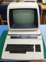
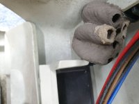
Acquired a 8032-SK that spend many years in a barn in a coastal city. This has caused a fair amount of corrosion on the IC pins that are socketed, to the point that many of the pins literally fall off. This is on top of the hornets nest inside the machine! :)

First order of the day was to remove the built-in bomb but, after doing that, no joy in booting it up. Did a few things:

1. I replaced the CPU and Character ROM that both lost pins (the pins literally fell off!) but the machine does not start.

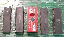
2. Installing one of Dave's (from Tynemouth) RAM/ROM replacement cards, and mapping everything out, gives the startup beeps but no display.

3. Looking at the video output signals, on the header connecting the monitor, I get H-sync but no V-Sync nor Video.

4. The RAM/ROM replacement card has a copy of (other) Dave's PETTESTER in it and if I select that, I get H-Sync and Video output but still no V-Sync.

5. I see the 7486 XOR that drives the video connector is socketed, so it looks like someone's worked on it before. Checking the input to the V-Sync XOR gate, shows no activity. So it seems the CRTC is not generating a V-Sync signal.


Any idea where to look next? Seems either the CRTC is not being set up or it's faulty?
Gary - Copy.jpg
Not a bad looking 8032-SK, taking into account it was in a barn for decades.
Hornets nest.jpg
Think the drivers that must operate the chips, all left.....
Gary-board.jpg
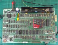
Universal board with a Tynemouth board installed, allowing it to boot - but no display.
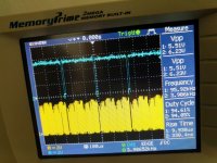
V-Sync Signal.jpg
Getting H-Sync (blue) and Video (yellow). This is with PETTESTER. Normal bootup gives H-Sync but nothing else.
 
The (other) Dave here...

Good detective work so far.

Yes, a socketed UC2 probably indicates that someone has been working on it as you have already guessed.

I assume you have already done this, but check the VSYNC output pin (40) from the CRTC itself UB13. If you have an open circuit PCB track (or a faulty connection) this may flush that out.

Power off and check for an accidental short circuit from UB13 pin 40 (VSYNC) to 0V or +5V. Or even a short circuit to anywhere else locally. If someone has worked on UC2 it could be there is a solder splash short circuit somewhere.

You could also try removing UC2 (as it is in a socket) and see what effect that has. I can see two (2) gates of IC2 used on schematic 10 of the UNIV2 - but not where the other two (2) gates are used.

It may also be worth scoping the other output pins of the CRTC (UB13) - TAn and RAn and see what you are getting.

Two possibilities then:

1. A dead CRTC.
2. The initialisation data is not getting to the CRTC correctly (corroded Dn pin on the CRTC). Again, check for continuity from the data pins of the CPU to the data pins of the CRTC.

Dave
 
Thanks Dave,

I need to figure out how to get to the CRTC with the Tynemouth RAM/ROM board plugged in as it obscures the CRTC.

As a quick check, I did pull the XOR from the socket but did not see any signals on the inputs of the XOR gate pins on the socket. Your idea to measure for shorts makes sense, will definitely do that.

What is interesting is that, if I boot with the normal ROMs enabled, I get H-Sync but no Video (in addition to not getting V-Sync). When I boot with the PETTESTER embedded in the TyneMouth ROM, I do get Video (but still no V-Sync). This seems to imply your PETTESTER somehow get the CRTC to generate video where the Edit ROM does not.

I also want to try your latest PETTESTER (V04, I think?) and see if I can configure the Tynemouth board to allow the PETTESTER to run from the Edit ROM socket and then check if it manages to configure the CRTC.
 
A further update on this;

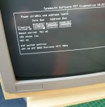
I switched to the Tynemouth PET Diagnostics board that plugs into the CPU sockets and exercise the 8032 board.

Checked for shorts, continuity, etc. Also reflowed the CRTC pins.

Still don't get V-Sync on pin-40 of the CRTC and also get no output on the RA0-RA4 outputs. These drive the lower 3 bits of the Character ROM address bus. The TA0-9 outputs do show data (at least on TA0-6) though.

Inputs to the CRTC does look right, it's getting Clock, Reset, CS, Data, etc.

Trying hard here not to have to take the CRTC out but it does seem to indicate a fault with the CRTC itself?
 
Another update.

I traced the circuit quite a bit and it does look like the CRTC should be set up but it is not successful. Some of the outputs of the CRTC seems dead, including the output pins that drive the Character ROM address lines. So I decided to replace it with a 6845 I pulled of an CGA card.

First question; Is the 6845 OK to be used on the 8032? From what I can read there are differences between it and the MOS 6545. But are these significant?

With the 6845 installed, I get the following:

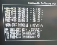
1. With the Tynemouth PET diagnostics board, I now get text output. :) It passes most of the RAM and fails all the ROMs. But I'm getting video output! :)
2. With the Tynemouth RAM/ROM replacement card (and everything mapped out), I get the startup tone but no text display. Both H and V-sync are present but no Video output. :(
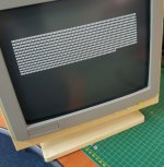
3. If I switch the RAM/ROM board to the inbuilt PETTESTER, I do get Video output.

Any idea what could be causing this? My understanding is that the diagnostics programs still use the video generation circuitry around the Character ROM, VRAM, etc.?

The new 6845 installed with the Tynemouth PET diagnostics
Tynemouth-1.jpg

Output text from the PET Diagnostics board
Tynemouth-2.jpg

PETTESTER on the Tynemouth RAM/ROM replacement board
PETTESTER.jpg
 
Yet another update (this is the 3rd update over the last few days but still awaiting the moderators to approve :( )

I found a socketed 6545 in another 8032 and tried that in Gary (the 8032 under repair).

Getting exactly the same symptoms, Video output with the diagnostics setups but no video output with just the system ROMs (via the Tynemouth RAM/ROM replacement board).
 
I see a whole load of approved posts now :)!

Keep posting, you’ll hit the ‘magic’ level before too long...

Your video circuitry is now working OK, as is your RAM.

The next thing to look at is why your ROM is faulty.

It looks like either every ROM is faulty (major bit rot) or the address decoder for the ROMs is faulty.

Looks like the CRTC was dead then.

Getting there...
 
I would check the inputs and outputs from UE12 (4 to 16 decoder).

It will be easier to use a NOP generator for this test.

It is also possible that one of the buffered address lines is faulty. Again, a NOP generator will prove or disprove this. However, for this to be true, it will depend on how clever the RAM test is at detecting an adress fault.

I can give you more information on how to perform this test if you wish. You need to identify the circuit for a 6502 NOP generator, or acquire a spare 6502, bend the eight data pins out and strap the to +5V or 0V (using low-valued resistors). A 6502 NOP is $EA = 1110 1010. 0 pins are connected to 0V and 1 pins are connected to +5V. 100 Ohm resistors should be good to use.

Dave
 
Yup, I think the problem might well be with the decoder. The Tynemouth PET diagnostic does a CRC 16 times per ROM and reports the CRC as 'inconsistent', i.e. it changes all the time. If I plug a new ROM into the Editor socket, it also reports as inconsistent.

Never played with a NOP Generator though I get a feel on how it will work. Going to Google a bit and see what I can do.
 
A bit of a side-story with more errors on this board :)

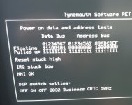
In addition to the inconsistent CRCs, I noticed the Tynemouth board also reported Reset stuck high and IRQ stuck low. It's also reporting RAM issues with the VRAM (and one can occasionally see random characters on the screen) but I'll fix that a bit later. Probably one of the 2114 chips.

The stuck Reset line, I traced to a faulty 555, and is now working properly. Quite cool that the PET diag board measures the reset timing. :)

The stuck IRQ is probably a bigger issue. From reading the circuit it seems the IRQ is driven by the VIA and two PIAs. So one of these chips is probably pulling this line low. Will go and sniff around them to see if I can see something but suspect I might have to socket them.

1. The IEEE PIA (UB16) is already on a socket and makes no difference if I pull it. IRO stays stuck low.
2. Getting the startup chirp so at least some of the VIA (UB15) must be working.
3. The Keyboard PIA (UB12) is the last one driving IRQ. Is there a way one can short a key and see if it generates an Interrupt?

Reset stuck high and IRQ stuck low.
IRQ Stuck.jpg

Reset fixed, now to look at that IRQ.
IRQ Stuck-2.jpg
 
Yet another thing broken on 'Gary' (and, mostly, another attempt to get to that magical approval-free 10 posts :) )

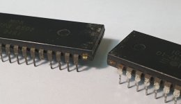
This 8032-SK lived in an outdoor shed for many years on the coast. Many of the pins of socketed IC have literally rusted off, especially on the 6502 and the Character ROM. The CPU I'll replace but thought to try and save the ROM, if possible, by Dremeling the pin open and soldering a new leg on.

Broken pins - 1.jpg

Broken pins - 2.jpg
 
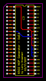
The trick is to use two sockets so that the NOP instruction pattern (1110 1010) is connected to the CPU chip only on the top socket, and the data lines (D7 thru D0) pins 26 thru 33 are open to the board circuitry on the bottom socket. In that way the CPU will happily execute NOPs all day while incrementing the address lines from $0000 to $FFFF. The CPU will then roll over to zero and start again. With a scope you can follow the square waves on the address lines. A0 will have the highest frequency of about 250 KHZ, A1 half of that, and A2 half of A1. If you spot something not in that pattern, you have found the problem. Note however that the RAM address inputs are multiplexed with the dynamic RAM refresh logic so it gets a little messy there. Hopefully with this method you will spot a bad buffer or whatever.


Also I would look at the eight data lines on the board (not at CPU) for shorted or open signals.

Here is a schematic from MikeS that shows all the pins straight thru from the top socket to the bottom socket except for the data lines that form the NOP code $EA (1110 1010).

6502_NOPpcb-ad5f77f0e6c0439f8e08cece619c407e.png
 
Last edited:
The trick is to use two sockets so that the NOP instruction pattern (1110 1010) is connected to the CPU chip only on the top socket, and the data lines (D7 thru D0) pins 26 thru 33 are open to the board circuitry on the bottom socket. In that way the CPU will happily execute NOPs all day while incrementing the address lines from $0000 to $FFFF. The CPU will then roll over to zero and start again. With a scope you can follow the square waves on the address lines. A0 will have the highest frequency of about 250 KHZ, A1 half of that, and A2 half of A1. If you spot something not in that pattern, you have found the problem. Note however that the RAM address inputs are multiplexed with the dynamic RAM refresh logic so it gets a little messy there. Hopefully with this method you will spot a bad buffer or whatever.


Also I would look at the eight data lines on the board (not at CPU) for shorted or open signals.

Thanks Dave, will definitely try that.

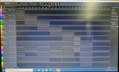
I plugged a logic analyser onto the inputs and outputs of the 74154 to try and see if the chip decodes the binary input correctly. This is while the Tynemouth Diagnostic board is doing the ROM CRCs. It selects the ROM one by one and does 16 reads to calculate the CRC of each. Because each ROM is tested 16 times, it's slightly more difficult (a lot actually :) ) to check if the logic is working, due to the 16 individual selects (see below), but it does seem so. There are 16 inverted CS pulses in the previous-selected ROM but I suspect it might be how the diagnostics board works as it's seen with all the chip-select lines. But it could also be wrong......See screenshot below.

It'll definitely be easier with clean signals with each address being read only once so I'm going to try the NOP method for sure. Love getting an excuse to build a new piece of test kit. :)

74154-3.jpg
 
A bit of a side-story with more errors on this board :)

In addition to the inconsistent CRCs, I noticed the Tynemouth board also reported Reset stuck high and IRQ stuck low. It's also reporting RAM issues with the VRAM (and one can occasionally see random characters on the screen) but I'll fix that a bit later. Probably one of the 2114 chips.

The stuck Reset line, I traced to a faulty 555, and is now working properly. Quite cool that the PET diag board measures the reset timing. :)

The stuck IRQ is probably a bigger issue. From reading the circuit it seems the IRQ is driven by the VIA and two PIAs. So one of these chips is probably pulling this line low. Will go and sniff around them to see if I can see something but suspect I might have to socket them.

1. The IEEE PIA (UB16) is already on a socket and makes no difference if I pull it. IRO stays stuck low.
2. Getting the startup chirp so at least some of the VIA (UB15) must be working.
3. The Keyboard PIA (UB12) is the last one driving IRQ. Is there a way one can short a key and see if it generates an Interrupt?

Reset stuck high and IRQ stuck low.
View attachment 63677

Reset fixed, now to look at that IRQ.
View attachment 63678

Looking at these screenshots, I just noticed now that D7 on the Data Bus did not pull high like it previously did. So, yet another problem to chase.
 
The trick is to use two sockets so that the NOP instruction pattern (1110 1010) is connected to the CPU chip only on the top socket, and the data lines (D7 thru D0) pins 26 thru 33 are open to the board circuitry on the bottom socket. In that way the CPU will happily execute NOPs all day while incrementing the address lines from $0000 to $FFFF. The CPU will then roll over to zero and start again. With a scope you can follow the square waves on the address lines. A0 will have the highest frequency of about 250 KHZ, A1 half of that, and A2 half of A1. If you spot something not in that pattern, you have found the problem. Note however that the RAM address inputs are multiplexed with the dynamic RAM refresh logic so it gets a little messy there. Hopefully with this method you will spot a bad buffer or whatever.


Also I would look at the eight data lines on the board (not at CPU) for shorted or open signals.

Here is a schematic from MikeS that shows all the pins straight thru from the top socket to the bottom socket except for the data lines that form the NOP code $EA (1110 1010).

View attachment 63692

I see this board straps the 6502 data bus directly to VCC and VSS while you indicated to use a 100ohm resistor per data line.

Would it be OK to strap the data bus directly to the supply lines?
 
Last edited:
My own 6502's NOP generator is also connecting the databus directly to VCC/VSS, so far I had no issues with it. However, in case some memory is permanently selected, it would kill it. I think the safe resistor value begins at 220 ohms however, and you need one resistor on each databus line to be safe.
I always check for RAM/ROM/IO chips clashing the databus before resorting to the NOP generator however (it's a kind of last chance on stubborn cases).

Frank IZ8DWF
 
My own 6502's NOP generator is also connecting the databus directly to VCC/VSS, so far I had no issues with it. However, in case some memory is permanently selected, it would kill it. I think the safe resistor value begins at 220 ohms however, and you need one resistor on each databus line to be safe.
Thanks Frank,

So, if the 6502 stays on 1 address and the data lines are strapped hard to supply, it can damage the CPU?
I always check for RAM/ROM/IO chips clashing the databus before resorting to the NOP generator however (it's a kind of last chance on stubborn cases).
Frank IZ8DWF
In this case, with the NOP generator, the CPU is disconnected from the data bus, it only exercises the address bus. If I read you correctly, you're saying that, by selecting chips on the data bus (via the stepping address bus), that could create problem. Can see that, yes.

How do you check for these clashed on the data bus? Just shorts to high and/or low?
 
The NOP generator disconnects the 6502 CPU data bus from the PET data bus and 'jams' a NOP instruction directly on the pins of the CPU.

No damage can, therefore, occur as a result of a data bus clash with the CPU.

In theory, no damage should occur to the CPU - as it should always be reading instructions from the data bus (with these being NOP instructions) with no data writes occurring.

It is just the 'engineer' in me that is abhorrent to tying things like this directly to VCC or 0V...

But, if push comes to shove, tying the data bus pins directly to VCC and 0V saves a few components, a bit of money and construction hassle - so why not. It is only a temporary measure for testing anyhow.

I once constructed an ETHERNET network from a bit of 2-core flex and a few 100 Ohm resistors for the terminators - bodge job or what (but I had no thicknet ethernet cable or terminators to use)!

If there are data bus clashes (e.g. one device trying to pull the data bus to +5V and another trying to pull the data bus to 0V) - then your oscilloscope should show you absolutely horrid waveforms that are neither at a logic '0' or a logic '1' level - but (possibly) somewhere in between. The story of the three bears - but in this case neither '1' or '0' is bad...

Dave
 
I once constructed an ETHERNET network from a bit of 2-core flex and a few 100 Ohm resistors for the terminators - bodge job or what (but I had no thicknet ethernet cable or terminators to use)!
Dave
With Z0 set correctly (like you did), the medium would not be an issue over short distances, so a perfectly acceptable hack. :)
 
Weekend, so time to work on this again. :)

Built a 6502 NOP Generator and it's a pretty cool tool!

All address signals directly on the CPU and after the first set of buffers (UD13, UD14) looks very clean. Will now start measuring deeper into the circuit. Any hints on where to sniff?

Then had a look at how UE12 is decoding the ROM select lines (see screenshot below) and the 154 seems to be working as expected. Need to look further for the inconsistent CRC report on all the ROMS.

I used two back to back tulip sockets and strapped the 6502 data lines directly to VSS and VCC
View attachment 63854
View attachment 63855

Measuring the input (A,B,C,D - the 4 bottom traces in the screenshot) and the ROM select lines (9 to F - top 7 signals) on the 74154.
View attachment 63856
 
Last edited:
Back
Top