ScottishColin
Experienced Member
I ran a test today for 9 hours on my 3016 just so none of you had to - I ran the PETTESTER v 04 ROM all day today to test speed and temperatures.
In summary, there were 267 RAM tests run in 9 hours which equates to 29.67 tests/hour (or pretty much 1 every two minutes).
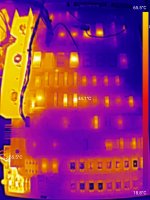
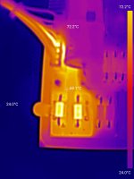
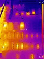
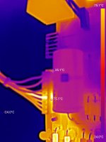
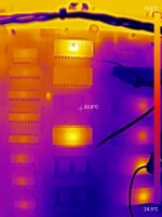
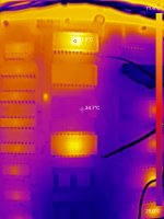
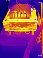
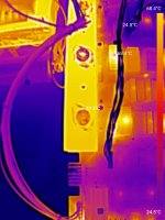
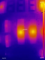
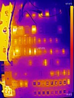
Here's a table of temperatures. Nothing was plugged into the PET - all devices were removed. It was running with the original 6502 and the BASIC v 2 ROMs (with the exception of the test ROM). UD7 has been replaced with an EPROM and I have the temperatures for that too (although they're not any different to the other ROMs).
The room temperature was measured as 19.8 c at the beginning. At all times expect when measurements were taken, the PET lid was closed and no keys were pressed.
The thing that piqued my interest was the difference in temperature between Row 2 (UI) of the RAM chips and row 1 (UJ) of the RAM chips - do the RAM tests exercise the UI row of RAM chips more than the UJ row?
I guess for this to even approach any kind of scientific rigour, I should load a 16K game and leave that running to see if there's a similar difference in temperature with that running too.
Any - this may well all mean nothing, especially with the number of replacement chips and sockets in my PET - but the RAM chips are the originals - any comments welcomed.
In summary, there were 267 RAM tests run in 9 hours which equates to 29.67 tests/hour (or pretty much 1 every two minutes).
Here's a table of temperatures. Nothing was plugged into the PET - all devices were removed. It was running with the original 6502 and the BASIC v 2 ROMs (with the exception of the test ROM). UD7 has been replaced with an EPROM and I have the temperatures for that too (although they're not any different to the other ROMs).
The room temperature was measured as 19.8 c at the beginning. At all times expect when measurements were taken, the PET lid was closed and no keys were pressed.
The thing that piqued my interest was the difference in temperature between Row 2 (UI) of the RAM chips and row 1 (UJ) of the RAM chips - do the RAM tests exercise the UI row of RAM chips more than the UJ row?
I guess for this to even approach any kind of scientific rigour, I should load a 16K game and leave that running to see if there's a similar difference in temperature with that running too.
Any - this may well all mean nothing, especially with the number of replacement chips and sockets in my PET - but the RAM chips are the originals - any comments welcomed.
| Device | Starting temperature | End temperature after 9 hours |
| 6502 (original chip) | 20.1 c | 31.9 c |
| UD6 (original chip) | 20.3 c | 37.0 c |
| UD8 (replacement - PETTESTER v04) | 21.3 c | 42.0 c |
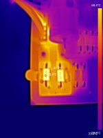
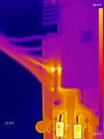
| Top of the transformer - original | 21.3 c | 44.2 c |
| Row 2 RAM (UI) - all original chips | 21.4 c | 36.7 c |
| Row 1 RAM (UJ) - all original chips | 21.2 c | 32.3 c |
| VR3 - original | 22.1 c | 45.6 c |
| VR4 - original | 22.0 c | 51.6 c |
| VR5 - original | 22.2 c | 49.7 c |
 . Yes, pun intended!