gwiley
Experienced Member
I’m excited to now have a PDP-8/M chassis for my system which was previously open-frame with a home-brew backplane and powered by lab supplies. I thought it might be interesting to share my experiences and benefit from the knowledge of experts in this group.
PDP-8/M chassis, freshly unboxed. Also in the box but not shown here is a bezel, two plexi panels and an extra power supply. It’s a bit dusty inside but the system components that I was missing are all here.
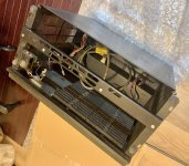
Chassis on the bench with cover removed and ready for disassembly, cleaning and testing.
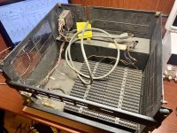
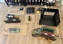
Key items are removed and most of them cleaned up. The backplane is only part way done. I need to borrow an air compressor to blow out the card slots. Bottom left is the spare supply board. Lower right is my present system with one of the new plexi panels resting over the KC8E programmer’s console. Interesting challenge here: KC8E is for an 8/E and I have an 8/M chassis. The KC8E that I have has incandescent bulbs but the chassis is wired for a panel with LEDs. I currently have a DC-DC module with digital meter to convert +15 to +8, and might stick that inside the chassis to power the lamps (the “yellow wire” to the KC8E) unless a better solution is possible.
Side note: I’m really more of a craft beer guy, but this is where we keep the wine. LOL
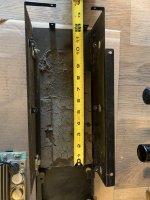
Measuring the power supply enclosure for new foam. The original foam had turned to dust. The old foam adhesive came off quite easily with a good coat of “Goo Gone”. Same with the foam on the inside of the top cover. A new roll of adhesive foam from Amazon is arriving today.
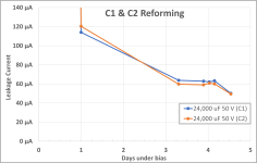
Reforming the electrolytic caps. This is the first time I’ve ever done this and have not had any experience using 45-year-old electrolytics. I searched quite a bit but was unable to find what I thought were rigorous technical papers on electrolytic reforming. However, there’s a lot of practical material available that was quite helpful. Present-day data sheets do provide formulas for leakage current as a function of capacitance and working voltage, so I had a ballpark target for the expected leakage. This was also an opportunity to characterize what happens in this process. I’ll share the data soon. I wish I had thought more about the reforming process in advance to be more methodical with data recording. This experience shows that the reforming process reduces leakage a lot.
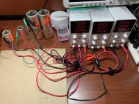
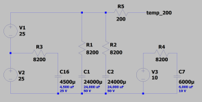
1. On the left is 6,000uF 10V (C7), connected through 8.2K to the 10V supply on the left.
2. Next is 4,500uF 25V (C14), connected through 8.2K to the middle supply.
3. 3 and 4 are 24,000uF 50V (C2 and C1), each connected through an 8.2K resistor to the two 25V supplies that are connected in series to get 50V.
There’s a tape-and-reel strip of 8.2K resistors in the garage, so that’s the reason for the value choice. It’s close to 10K which I was looking for.
I’ve now put the two output caps (the smaller ones, C7 and C14) back on the power supply board and started testing it under load. This preliminary test is powered by a lab supply; haven't yet connected the transformer. So far so good. It seems pretty robust so far. The -15V and +15V are solid up to 8A and 1A, respectively, and a little beyond. I’ve only loaded the +5V output with a few amps so far. After watching Jerry Walker’s video on this topic and it’s clear that the +5V output needs to be fully loaded before victory is declared. I can share the load regulation and efficiency data soon.
PDP-8/M chassis, freshly unboxed. Also in the box but not shown here is a bezel, two plexi panels and an extra power supply. It’s a bit dusty inside but the system components that I was missing are all here.

Chassis on the bench with cover removed and ready for disassembly, cleaning and testing.

Key items are removed and most of them cleaned up. The backplane is only part way done. I need to borrow an air compressor to blow out the card slots. Bottom left is the spare supply board. Lower right is my present system with one of the new plexi panels resting over the KC8E programmer’s console. Interesting challenge here: KC8E is for an 8/E and I have an 8/M chassis. The KC8E that I have has incandescent bulbs but the chassis is wired for a panel with LEDs. I currently have a DC-DC module with digital meter to convert +15 to +8, and might stick that inside the chassis to power the lamps (the “yellow wire” to the KC8E) unless a better solution is possible.
Side note: I’m really more of a craft beer guy, but this is where we keep the wine. LOL

Measuring the power supply enclosure for new foam. The original foam had turned to dust. The old foam adhesive came off quite easily with a good coat of “Goo Gone”. Same with the foam on the inside of the top cover. A new roll of adhesive foam from Amazon is arriving today.

Reforming the electrolytic caps. This is the first time I’ve ever done this and have not had any experience using 45-year-old electrolytics. I searched quite a bit but was unable to find what I thought were rigorous technical papers on electrolytic reforming. However, there’s a lot of practical material available that was quite helpful. Present-day data sheets do provide formulas for leakage current as a function of capacitance and working voltage, so I had a ballpark target for the expected leakage. This was also an opportunity to characterize what happens in this process. I’ll share the data soon. I wish I had thought more about the reforming process in advance to be more methodical with data recording. This experience shows that the reforming process reduces leakage a lot.

1. On the left is 6,000uF 10V (C7), connected through 8.2K to the 10V supply on the left.
2. Next is 4,500uF 25V (C14), connected through 8.2K to the middle supply.
3. 3 and 4 are 24,000uF 50V (C2 and C1), each connected through an 8.2K resistor to the two 25V supplies that are connected in series to get 50V.
There’s a tape-and-reel strip of 8.2K resistors in the garage, so that’s the reason for the value choice. It’s close to 10K which I was looking for.
I’ve now put the two output caps (the smaller ones, C7 and C14) back on the power supply board and started testing it under load. This preliminary test is powered by a lab supply; haven't yet connected the transformer. So far so good. It seems pretty robust so far. The -15V and +15V are solid up to 8A and 1A, respectively, and a little beyond. I’ve only loaded the +5V output with a few amps so far. After watching Jerry Walker’s video on this topic and it’s clear that the +5V output needs to be fully loaded before victory is declared. I can share the load regulation and efficiency data soon.

