stepleton
Veteran Member
I think this is a fairly basic electronics question.
If you read datasheets for old DRAMs that used multiple power supplies, you'll find warnings like these:

That's "Forward biasing this supply (that's Vbb) with respect to Vss will destroy the memory device". You'll also find instructions like the last line here:
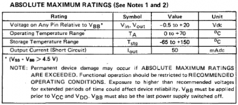
"Vbb must be applied prior to Vcc and Vdd. Vbb must also be the last power supply switched off."
Mostek at least did you the courtesy of explaining the reason for this (although surely many readers of the datasheet would have known it anyway), and they also gave you perhaps a bit more leeway with some of their devices:

"The Vbb supply is an extremely important 'protective voltage' since it performs two essential functions within the device. It establishes proper junction isolation and sets field-effect thresholds, both thin field and thick field." Plus more about how you can leave Vbb at 0V for around five seconds.
My question is: what kinds of techniques did system designers use to make sure that they were ready with the reverse bias voltage before the other rails came up? I'm thinking in particular of S100 cards like this one:
http://www.s100computers.com/Hardware Folder/Dynabyte/16K DRAM/16K DRAM.htm
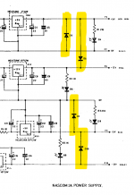
where it looks like you just have a bunch of voltage regulators and not a whole lot of machinery there dedicated to power supply power-up sequencing, at least that I can find. (Was there any?) Did you find other precautions, like fitting a nominally reverse-biased diode so that Vbb could never exceed Vdd?
If you read datasheets for old DRAMs that used multiple power supplies, you'll find warnings like these:

That's "Forward biasing this supply (that's Vbb) with respect to Vss will destroy the memory device". You'll also find instructions like the last line here:

"Vbb must be applied prior to Vcc and Vdd. Vbb must also be the last power supply switched off."
Mostek at least did you the courtesy of explaining the reason for this (although surely many readers of the datasheet would have known it anyway), and they also gave you perhaps a bit more leeway with some of their devices:

"The Vbb supply is an extremely important 'protective voltage' since it performs two essential functions within the device. It establishes proper junction isolation and sets field-effect thresholds, both thin field and thick field." Plus more about how you can leave Vbb at 0V for around five seconds.
My question is: what kinds of techniques did system designers use to make sure that they were ready with the reverse bias voltage before the other rails came up? I'm thinking in particular of S100 cards like this one:
http://www.s100computers.com/Hardware Folder/Dynabyte/16K DRAM/16K DRAM.htm
where it looks like you just have a bunch of voltage regulators and not a whole lot of machinery there dedicated to power supply power-up sequencing, at least that I can find. (Was there any?) Did you find other precautions, like fitting a nominally reverse-biased diode so that Vbb could never exceed Vdd?

