• Please review our updated Terms and Rules here

How to build internal 3kB memory expansion for VIC 20?

VintageVic

Experienced Member
Joined
Dec 9, 2019
Messages
340
Location
Finland
Okay,

so I have a couple of MB 8128-15 (2kBx8) RAM chips and I can pull one more from donor 1541 pcb.
Question is, how to build 3kB memory expansion for the Vic?

Best approach I believe, is to use expansion slot pins to make connections. These I mean:

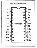
I've attached MB8128 pinout here. I suppose I will connect:
- A0 - A10 pins to the Address bus
- I/O 1 - I/O 8 to the data bus
- gnd and Vcc are obvious...
- pin 18CS to the expansion slot pin 14 (RAM1), pin 15 (for RAM2) and pin 16 (for RAM3)

but... what about pins 20 OutputEnable and 21 WriteEnable for each chip?
I guess I need one (or more) logic chip(s) that checks for instance if RAM1 CS is high then
it makes either WE or OE high on RAM1 depending on how CPU R/W is set (at expansion slot pin 18)?

I could probably figure this out on my own too... being first timer I'd be making things too complicated.
This must have already been figured out, so if you know, please share your knowledge here :).

Also, I'd like to add on/off switch to run software that are made for unexpanded VIC. I guess simpliest
solution is to cut power for all chips at pin 24 for this purpose.

Notes:
I know I will be wasting the extra 1kb ram on each chip, since these are 2kb chips. It does not matter,
since I have these memory chips to use at my disposal.

I have already tried and succeeded to make 32kb ram expansion for blocks 1-5 using instructions
found online. I now want to learn how to add this 3kB extra.
 

Attachments

  • Pin_MB8128-15.jpg
    Pin_MB8128-15.jpg
    26.8 KB · Views: 2
Right then, first partial plan for logic connections for RAM1 chip, using
7408 AND gate and 7404 hex inverter to get desired outputs for RAM1 OE and WE pins.

Does this look like it could work for the logic part?

I'll draw more complete design that also includes RAM2, RAM3. I'll be needing two 7408 ic's, but one hex inverter
should be enough for all of the RAMs. Perhaps there is simpler solution that just did not occur to me?
 

Attachments

  • RAM_plan.jpg
    RAM_plan.jpg
    95.6 KB · Views: 11
Are you really stuck on using the salvaged 2K chips? If you want to do this as minimally as possible maybe it'd make more sense to get a single larger chip. (You can get an 8kx8 or 32kx8 SRAM for around $4.)

My off-the-cuff suggestion for a minimal circuit would be a single 4K or bigger RAM chip plus a single 74LS10 triple 3-input NAND gate. Wire RAM1-3 to the inputs of one gate. The output of that gate should go high when any of the three RAM lines is selected. Feed that signal back into a second NAND gate, and tie the other two lines to a 10K-ish pull-up resistor connected to 5v, and a switch going to ground. When the switch is open the second gate will act like an inverter, giving you the active-low chip select for your RAM chip; when the switch is closed and pulls the other inputs low it'll act as a disable switch for the memory expansion. On the RAM chip you'll need A0-A11, tie the remaining lines high or low, doesn't really matter. I'm also *reasonably* sure that on most RAM chips you don't need to worry about gating OE on WE, you can just tie your chip enable to both CE and OE and if write is active it takes priority.

nand.jpg

If you really want to use the old 2K chips then use two of them, not three, and instead of the 74LS10 use a 74LS00 quad NAND gate. I think this schematic will work to give you two switchable chip selects; one is just a switched version of RAM1 and the other is a combined RAM2/3.

nand2.jpg

Note that I don't guaruntee any of these suggestions, it's very possible I haven't had enough coffee and inverted the truth table somewhere, but conceptually I think the theory is sound.

I would not recommend trying to just cutting off the power to disable the RAM. Weird stuff can happen with unpowered chips hanging on the bus; in some cases you can actually end up with them partially working because of them drawing power parasitically through the signal lines, which is bad for everyone involved.
 
I have already tried and succeeded to make 32kb ram expansion for blocks 1-5 using instructions
found online. I now want to learn how to add this 3kB extra.

Out of curiosity, what design did you use for this? If you did a design using a single 62256 or similar chip (like this one?) maybe you could just piggyback another 62256 on top of it (all pins matching except OE and CE, bend those two up vertical), attach a 7410 NAND gate to RAM1-RAM3 like I suggest above, and tie the chip select output to the OE/CE pins. You'll be wasting 29K of the second 62256, but they effectively cost the same as or less than 6264s so who cares?

(Also, FWIW, maybe that "powered" disable in that schematic was overly complicated. To make it even easier, use a 74LS11 AND instead of the NAND, put the disable switch directly on the chip select signal, and just put a 10k pull-up resistor on the memory chip side of it.)
 
Thanks for the assistance and suggestions!

No, I'm not stuck on using salvaged chips. I'm still beginner in hardware hacking, that partial schematic I drew above
was my very first own design to solve a problem. I actually thought that I need to have three ram chips to make this work.

This is why it's great to ask questions here - there was immediately more clever way to approach the problem!
Yes, you guessed it, I used that design by Adam Bergström you linked above. By the way Adam, if you read this, thanks to you as well
for that!

The simpliest way probably is to piggybag second 62256 chip on top of the other and go on from there.
I'll probably try that.

Yet, I have more Vic's. It could be fun project for me to try out with the salvaged 2kB chips. If nothing else - to prove
myself I was able to do that!

Using two of these is clearly more clever way. I think I have to redraw your scetch to include logic chips and their pins to get
a good idea how to implement it.
 
Giobbi, thanks for this suggestion as well.

I have also tried Per Olofssons hack to the letter. I still have that VIC, with 16k added RAM, without
your mod to increase it to 32k RAM.

However, my point was to know/learn how to add this additional 3kB RAM internally to the VIC.
There aren't many programs that require additional 35kB, but one comes to mind, the "Doom" port for
the VIC that does. Still for me it is probably more interesting to learn how to make this hack rather than
actually using it.
 
> My off-the-cuff suggestion for a minimal circuit would be a single 4K or bigger RAM chip plus a single 74LS10 triple 3-input NAND gate.
> Wire RAM1-3 to the inputs of one gate. The output of that gate should go high when any of the three RAM lines is selected.

Okay, I've been scratching my head trying to figure out the logic of this suggestion.
If I wire RAM1-3 to the inputs of 3-input NAND gate, it is correct that the output is HIGH, if any of tha RAM1-3 is high.
But isn't it a problem, that if all RAM1-3 are low --> NAND gate output is still high?

This then would result that if any of RAM1-3 are high or low, regardless the first 3-input NAND gate output is always high resulting the second
3-input NAND gate always to be low. Thus CS/OE of the RAM chip would always be low?

In fact, RAM1-3 are never simultaneously high (or are they?). If all RAM1-3 were high then 3-input NAND gate would output a low.

Perhaps my logic is wrong here, but I'd like second opinion on this?

Edit:
Hey - if we replace 3-input NAND gate with 3-input OR gate (say M74HC4075) then the suggested logic
seems to work ! With all RAM1-3 low - output equals low. But if any of the RAM1-3 goes high, the output of
the OR gate also goes high.

Also, shouldn't I need to feed that output to 3-input AND gate to include pull-up resistor and switch.
Then when one of the RAM1-3 is high AND the switch is open the AND gate outputs high enabling the RAM chip?

This now needs two logic chips and is getting a bit more complicated. But is the logic sound?
 
Last edited:
This then would result that if any of RAM1-3 are high or low, regardless the first 3-input NAND gate output is always high resulting the second
3-input NAND gate always to be low. Thus CS/OE of the RAM chip would always be low?

Here's the function table of a 74LS10:
ABCY
xxLH
xLxH
LxxH
HHHL

IE, if all inputs are high the output is low. The RAM1-3 outputs are active low, so if none of them are active the output of the '11 will be low, while if any of them are active the output will be high. So this does what we want, IE, it gives us a chip select that will change state if any of the RAM1-3 outputs are active, but, yes, it's active the wrong direction because the RAM chip wants an active LOW on CE/OE. So...


That's why the output from the first NAND gate is channeled through the second one. In the schematic I have a pull-up (thus creating an "H" on two of the inputs); this turns the second NAND gate into a simple inverter; an "H", IE, active (H) state from the "decoder" NAND fed into the third gate is turned into an "L", and an inactive (L) state is turned into an "H". The memory disable function is implemented by adding a switch that grounds the two inputs connected to the pull-up; that will make those two inputs always "L", which means the output will always be "H".

Basically the thing you "get" out of doing it this way is the disable switch isn't directly in line with the memory select, which might make it a little more immune to noise. (The second NAND gate is basically acting as an inverting buffer with an output enable.) Realistically it's probably fine to just use a 74LS11 instead; its function table will look the same as the above except the output isn't inverting:


ABCY
xxLL
xLxL
LxxL
HHHH

IE, if any input is low the output is low. With this you don't need a second gate as switchable inverter, you put the memory disable switch between the output of the decoder and a pull-up resistor connected to the OE/CE lines.

For the schematic using two RAM chips the NAND version has, in addition to the possible additional noise resistance of not putting the RAM enable lines through a switch, the advantage that you don't need a double-pole switch to disable both RAM chips, a single pole that grounds the pull-up holding the extra gates high on both switchable inverters does the job for the whole circuit.
 
Hey - if we replace 3-input NAND gate with 3-input OR gate (say M74HC4075) then the suggested logic
seems to work ! With all RAM1-3 low - output equals low. But if any of the RAM1-3 goes high, the output of
the OR gate also goes high.

.... oh.

Just to clarify the above a little more, in the VIC-20 schematic I looked at RAM1-3 all had a line over the top of them. That generally denotes "active low". (FWIW, this is almost universal when it comes to chip select signals. Active=Low, not High.) So an OR gate is definitely *not* what you want. Unless something is broken on your VIC-20 more than one of the RAM* lines should *never* be low at the same time.
 
To keep things simple you can use the character ROM socket. It has all but two of the signals you need. I did this with my 8kinside project, which places a TSOP 6264 8k SRAM underneath the character ROM.
The tricks are few: Tie VA13 to CS (active high, pin 26 on the SRAM) right on the ROM socket, /BLK0 from UC4 /G2, and VR/W from any of the internal ram chips. You'll have to somehow disable UC4 as well, as any assertion of /ram0 to /ram7 will trigger the big memory switch 74ls133 and override the mapping of the 8k internal ram by taking the cpu off the video bus. I did this in prototype by removing UC4 and setting its outputs high, but ultimately put a switch to select the signal from /G2 on UC4 or to the 8kinside memory. I cut the leg of UC4 at the PCB (rather than cut the PCB!) and soldered a jumper block to it to switch back and forth in the end. I rarely don't have this enabled since external 3k ram carts are unnecessary and overridden, and it's easy enough to change the memory map with a few pokes and a new.

The neatest thing about this is now the RAM at 1024-4095 is accessible by the video chip, so you can put the screen at 1024 and see a spacious '31231 BYTES FREE' with a full load of RAM from 0-32767. I patched a basic4 ROM to set this up for me automatically. The KENRAL won't do this as it's written to assume the memory below 4096 and above 1023 are not accessible to the video chip.

Unfortunately this was done direct to PCB in Eagle, so I don't have a schematic.

Forgive the prototype on the expansion port in the running picture; it's an ISP KERNAL prototype. :ninja:

For anyone that likes hardware, figure out why I used va13=high to enable the SRAM even though the CPU sees it at 0-8191 :)
 

Attachments

  • 8192-inside.jpg
    8192-inside.jpg
    520.6 KB · Views: 13
  • 4--pass.jpg
    4--pass.jpg
    712.5 KB · Views: 13
Thanks for correcting me out, Eudimorphodon. That active low had me confused. I always
wrongfully assumed all RAM1-3 signals are low until any ram is accessed. Furthermore, I thought
CS/OE must be low until ram chip is accessed and not vice versa.

I think I learned something here. It's nicer to know how things work instead of just building a project
without understanding its operational principles.

Very cool and neat looking project jbevren!
 
For anyone that likes hardware, figure out why I used va13=high to enable the SRAM even though the CPU sees it at 0-8191

I’m going to resist the urge to confirm my answer with googling and just go with my guess based on the schematic: based on the wiring of the character ROM and G1 on that 74138 to VA13 that the VIC chip’s default memory map is topsy-turvy compared to the computer as a whole. (Character ROM on the bottom half of the total 16k available, RAM on the top. VA13 is directly used as a chip select either direction.)
 
I’m going to resist the urge to confirm my answer with googling and just go with my guess based on the schematic: based on the wiring of the character ROM and G1 on that 74138 to VA13 that the VIC chip’s default memory map is topsy-turvy compared to the computer as a whole. (Character ROM on the bottom half of the total 16k available, RAM on the top. VA13 is directly used as a chip select either direction.)
Exactly! This had to be done as the vic chip is hardwired in silicon to respond to address 4096 (as noted vaguely in the datasheet). It boggled me for a long while that the VIC chip has no chip-select input. Flipping the address map around can also be confirmed by the 'default' character memory address being at 0 according to the registers in the VIC chip. This is caused by BLK4's output being routed to VA13 through UE8 by the way.

The vic-20 logic is simple on the surface but has a few surprising twists in it for sure. :)
 
It boggled me for a long while that the VIC chip has no chip-select input.

Yeah, it's confusing. Honestly I still haven't completely wrapped my head around the clock-phase bus structure of the 6500 family chips and how it makes quite a few things... implicit rather than explicit. ("Explicit" in the way they are on 8080-descended buses, anyway.)
 
The neatest thing about this is now the RAM at 1024-4095 is accessible by the video chip, so you can put the screen at 1024 and see a spacious '31231 BYTES FREE' with a full load of RAM from 0-32767.
...
The vic-20 logic is simple on the surface but has a few surprising twists in it for sure. :)

I've been mulling this over a while and I'm actually a little bit baffled why Commodore didn't use the "VA" address lines and "BD" data lines on the cartridge port instead of the CPU-only "C" lines. If they'd been clever they could have made it possible for cartridge memory to be read directly from the VIC chip. This not only would have enabled 8K of RAM to be directly addressed by the VIC at the low end of the memory map, I *think* they also could have allowed an additional 4K character/glyph ROM to be read at an effective position of 1000 by the VIC chip during the part of the cycle when it owns the bus; this ROM would be invisible to the CPU of course, it'd see I/O in its 9000 position per usual.

The other thing I'll never get about the VIC is why in the world they left that 3K hole in the memory map instead of just putting the other RAM chips directly above the first 1K.
 
The VA and BD lines are probably not extended to the cart port due to load limitations of the VIC chip. That's pure guesswork on my part. That, and the video address bus is only 14 bits. :p

The 3k hole I think is an economical decision made with the end user in mind. Here's a theory of mine: When the Vic-20 was released, ram was prohibitively expensive and BASIC requires contiguous memory to operate correctly. Without the 3k hole, the user would have to somehow use a 3k cartridge at the same time as an 8k cartridge to get more than 6k of ram available to BASIC. This means a bus board and buying two carts are required for one memory expansion. With the 3k hole in a lower memory location you can add 3k or 8k without worrying about losing available memory or having to stack addons to get what you need done.

The KERNAL could consider moving BASIC to the beginning of the new 8k memory if there's a hole above the onboard 3k, but you're throwing 3k of memory away, which would be considered very wasteful in the day.
 
The VA and BD lines are probably not extended to the cart port due to load limitations of the VIC chip. That's pure guesswork on my part. That, and the video address bus is only 14 bits. :p

But the cartridge port is also only 14 bits. ;) Considering how they already broke the memory map into 8k blocks a scheme that leveraged VA13 as a “high/low” signal as it already is internally and just used 13 address lines would have worked just as well.

That whole deal with settling on 5k was frankly pretty goofy. I guess the story supposedly was that they had a huge surplus of the 1kx4 SRAMs just lying around or whatever, but choosing to use *10* of them instead of 16 (or 8, for that matter) was just… okay, sure.

Anyway, easy fix is just to sell 3k and 11k cartridges instead of 3k and 8k, right? ;)
 
Dividing the memory into 8k blocks makes it easier to build a ram or rom cartridge. With a 6264 or similar static ram all you have to do is hook up vr/w, a BLK signal, address, and data bits for example.
I'd personally prefer the whole address bus, but in an era where ram was expensive and logic chips were starting to get hard to find this is pretty sensible.
 
Back
Top