• Please review our updated Terms and Rules here

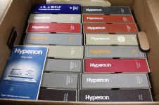
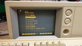
I walked into a junk shop and walked out with a Dynalogic Hyperion!

It's definitely glued together. Perhaps one day I will open it up but it will likely crack the case so that's why I have not done so.

FWIW, looking at the technical manual for the system there's pinout for the "EX connector" on the back, and it looks like it's a mostly complete subset of the ISA bus signals. I don't see any deal-breakers for banging together a simple SRAM-based memory expansion. The "only" confusing part is the meaning/use of the "EX PORT 213H". Basically the Hyperion appears to have a subset of the interface card IBM used to talk to the 5161 expansion chassis in front of that bus connector, and it's not entirely clear how that's decoded/used to read the memory size switches in the expansion chassis (or if that's strictly necessary to make it work), and/or if there's some kind of "presence detect" that needs to be fulfilled.

The pinout doesn't seem to have an obvious "this being grounded means the chassis is present" line, nor one to indicate a configuration read operation. I wonder if it expects you to decode port 213h in anything that plugs into this slot and pass through the switch/jumper state(*), or if that might be "optional" and a RAM-only expansion can get away with just decoding the port like it would a normal bus. I guess, just for laughs... if you have a working Hyperion, does reading port 213h with an "IN" command return a different value depending on if the memory expansion is plugged in or not?

(* The expansion module "plug and play" of the IBM Convertible actually works something like this. It's kind of insidious because IBM implemented it by putting a proprietary custom chip in every peripheral. It's not that complicated, you could mostly fake it it with a GAL, but it's still gross.)
 
... Another note about the Hyperion from reading the manual, it *kinda* looks to me like the BIOS doesn't read BIOS extensions, so making a hard disk (IE, XT-IDE or whatever) add-on directly bootable might be non-trivial? If I'm reading it correctly the manual basically says to use Hyperion's own expansion-chassis hard-disk add-on you had to patch IO.SYS on your boot floppy?
 
I don't see any deal-breakers for banging together a simple SRAM-based memory expansion.
That's cool. Some of what you said goes over my meatball technician's head, but for some stupid reason it didn't even occur to me to look to the rear interface for a pseudo-ISA slot interface prospect. Duh.

One thing I was wondering though. My Eagle Spirit luggable PC of the same era originally came with 256K, as 4 banks of 4164 chips. The first two were soldered in, and the latter two were socketed. In accordance with the manual, I swapped out the 16 socketed chips for 41256's (expensive at the time!), and closed one jumper, which brought my Eagle to its maximum 640K. (In fact, back at that humble computer beginning I didn't even have a spare jumper, and had to fashion one out of a perverted paper clip!)

I wonder if the design of the Hyperion allows for such a scenario, even if the soldered-in chips, (9 per bank with parity), makes the effort rather more daunting.
 
I wonder if the design of the Hyperion allows for such a scenario, even if the soldered-in chips, (9 per bank with parity), makes the effort rather more daunting.

Volume 2 of the maintenance manual has schematics, and I think I see a hard deal-breaker for swapping in denser chips: the schematic says it uses an AM2964B DRAM controller. (Which is interesting, that means it's not following the IBM example of having the DMA controller do memory refresh.) That chip is literally hardwired to do a max of 4 banks of DRAM, and the maximum size of the banks is 64K. (The address bus from the CPU is 16 bits plus two bank select lines for 18 bits, and there are eight multiplexed address lines on the DRAM side.) There's no straightforward way to make this support 256K per bank; if it used discrete parts you could hack it, but all the moving parts live inside that DRAM controller chip.
 
The address bus from the CPU is 16 bits plus two bank select lines for 18 bits, and there are eight multiplexed address lines on the DRAM side.

I tip my hat to anyone that familiar with the chips and who can read a schematic to that level of understanding.

I can't. Oh my hobby skills improve over time, so I become "confused at a higher level", but to my poor eyesight the address and data lines still cross and blur and feel like something just out of reach. Salute, Sir.
 
A small request for @TMA-1, @snuci, or anyone else with a working Hyperion:

- Do you happen to have dumps of the character ROM on this thing, by any chance?
- Alternatively: would you be willing to run a small program (which I will provide) and take some decent photos of the screen output?

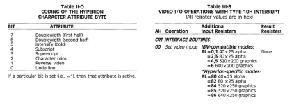
I ask since this thing seems to have some neat text and video capabilities:

hyptxt.png

Bitmap typography on these oldschool machines is often overlooked... it'd be cool to study how this works and what it actually looks like, and maybe make an addition to this project.
 
@VileR, check here: https://vintagecomputer.ca/files/Dynalogic Hyperion/firmware/https://vintagecomputer.ca/files/Dynalogic Hyperion/firmware/

I just uploaded it. I didn't realize I didn't have it up there already.

Hope this helps,
Santo

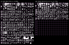
it sure does - much obliged! I was able to extract the charsets for the 250-line (native) and 200-line ("IBM") modes.

Although now I'm curious how the subscript and superscript attributes are implemented. I thought there would be separate smaller bitmaps for those, but there aren't. Maybe the text editor ("IN:SCRIBE") has a way of showing that off?

hypchars.png
 
Nice! Thanks for the demonstration... yeah, it looks like the sub/superscript attributes act as modifiers for the chargen ROM address, adding/subtracting a byte or two as necessary to shift the characters. I guess it helps that the ROM stores 16 lines per character, with the final six being blank, so that little hack doesn't result in garbage.
 
In a number of ways this is a pretty interesting machine; it's kind of remarkable how PC Compatible it manages to be despite using different chips for a lot of functions. (For instance, the SMC 9007 CRT controller instead of a 6845; the character attributes it has in "Hyperion" mode are applied using an SMC 8021-003 VAC.) I mean, in a vacuum there's nothing *wrong* with how anything was implemented on it, using the DRAM controller, for instance, saves a lot of finicky moving parts... it's just "different" in ways that PC software is likely to trip over if it really tickles the machine's innards.

The BIOS apparently manages to cover up a lot of sins, and its memory map at least is PC compatible, which is basically what saves this from being completely consigned to the "MS-DOS Compatible" bucket like a Tandy 2000 or something. Using the Zilog chip for the serial UART was probably their biggest misfire... which, again, if it wasn't for the fact that so much software insists on poking the guts in off-limits areas should have been fine. Not their fault that the PC serial bios routines suck so badly nobody wanted to use them, right?

Running 8088 MPH or Area 5150 isn't going to be happening, that's for sure. ;)
 
Last edited:
Back
Top