• Please review our updated Terms and Rules here

Imsai 8080 cannot examine to RAM adress...

Sorry, i was on the false pin with psync. I have to say, i bought the logic analyzer before a few weeks and it´s the first time to work with it.. :) I´ll now check again the databus. Psync goes from low to high and not from high to low. What do you think about that ?

View attachment 56504

So, C3 and the MSB and LSB are there. I think, there is something wrong in the 8t97 area ?!

THX

Jan

I think it was an error in the drawing. It is a PSYNC\ so falling signal is correct as you are seeing. I posted before you. Are you saying you see the correct C3 and address bits on the data lines? It is PSYNC positive on the mother board.It is inverted once to U13-8.
Dwight
 
Hello.

Ok. But now, i damaged the plug from the flat cable to the cpu board. I ordered a new one. When it is installed i´ll check the things you said.

THX

Jan
 
Hello.

Ok. But now, i damaged the plug from the flat cable to the cpu board. I ordered a new one. When it is installed i´ll check the things you said.

THX

Jan

You can disconnect the cable with the CPU card in place and run the test I asked for. In fact, I think we can complete the diagnosis. At most, you will need some wire and a few resistors of about 2K to 5K someplace and maybe some some 1K resistors.
I may need to know which CPU card you have? We are really close to solving it don't quit now. You can replace the cable later.
Dwight
 
Last edited:
So, i checked something. There are cables on the back of the pcb. I checked them with manual, they are correctly !

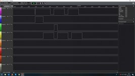
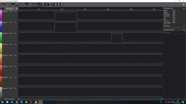
Then, i made your measurement. I switched on the imsai and pushed examine.

CH0 = U18 - 12
CH1 = U10 - 12
CH2 = U12 - 8
CH3 = U14 - 6
GND = U10 - 7

imsai_no_examine2.jpg


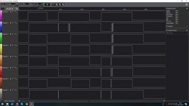
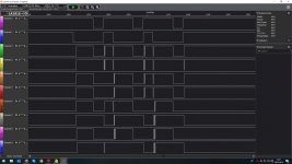
Then i connected logic analyzer to Databit 0 - Databit 7 on the CPU-card.

CH0 = Bit 0
CH1 = Bit 1
CH2 = Bit 2
CH3 = Bit 3
CH4 = Bit 4
CH5 = Bit 5
CH6 = Bit 6
CH7 = Bit 7
GND = CPU GND Pin 2

data_bits_while_examine.jpg

I switched on imsai and pushed examine. I have set the adress to 00F0h. So, the 4 switches on the left side of the right side switches were up before starting. The Imsai makes something, but not the right steps. It does not look like 00 C3 00 F0.


My CPU card is a MPU-A Rev-4

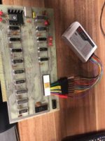
Please take a look to the picture:

MPU-A.jpg


I swapped the 5 7405 behind the adress switches. No changes. What do you think ?

THX

Jan
 
The first set of values look really strange. First, just to make sure, you are triggering on channel 0 only.
It looks like something is wrong in the decoder but I can't make sense yet.
The data pins will look funny because there is a number of things going on, including CPU status. You have to have a channel connected to pDBIN as the value from the front panel is only valid while pDBIN is positive and even then the leading edge may be a little off. There should be 3 pulses of pDBIN, depending on what instruction it thinks it is doing( in other words C3 ).
The first set of data is so wild, I'd like you to measure the following:
channel 0 = U10-12
channel 1 = U6-3
channel 2 = U7-1
channel 3 = U4-9
Trigger on channel 0
The same thing, hit examine.
Dwight
 
Can you also verify that U11 and U12 are the correct devices?
U12 should be a 7410 and U11 should be a 74LS10.
I'm trying to figure how you could get the signals you were getting given the state of pDBIN. U14-6 looks like what U13-6 should look like. Are you sure you were on the right pins?? The other two signals looked right but U14-6 looked wrong?????
Dwight
 
Last edited:
Looking at the first logic analyzer picture on post $41

I'm going to go forward with assuming Ch3 was probing the wron chip and was looking at U13-6. Even if it wasn't on that pin, we can see that the strobe for the C3 was correct in the picture. We just need to understand why it didn't get through.
This would mean the signal is really the inverse of pDBIN.
The processor samples the data pins on the falling edge of the pDBIN signal, or in this display, the rising edge as it is inverted in the picture.
It would seem that we have a number of possible problems.
The logic is creating the correct emable to the 7405s for the C3 signal.
Instead of the logic levels, I'd said we should probe in the previous post, I'd like to see the following:

Ch0 = pSYNC
Ch1 = U11-3
Ch2 = D0
Ch3 = D1
Ch4 = D2
Ch5 = D3
Ch6 = D4
Ch7 = D5

Later we can swap D4 and D5 for D6 and D7. pSYNC will give us a known starting point and U11-3 will give us reference edged to determine what data the processor was receiving as input.
Dwight
 
Hello.

I checked again the pin´s from your schematic. Now, every signal is fine. Take a look:

imsai_no_examine3.jpg

Then, today i´ve got my ordering of logic chips and my new plug for the flat cable. I swapped all logic chips on frontpanel except 8T97N and 7427. One by one. But no changes. I cannot examine memory adress. I checked again every chip on frontpanel and on mpu-a card for right positioning. Everything fine !

When i am on memory adress 00. I switched with the toggles C3 00 F0 and reset and made "single step" for three times. It jumps to memory adress F000, the 4 LED´s on the left side are on. So, there should not be any trouble with MPU-A card ?!

I made your other measurement, expat U4-9. I have no access to this pin, i would have to desolder a toggle switch.

imsai_no_examine4.jpg


THX for your help !

Jan
 
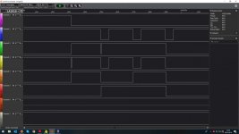
So, i made also the measurement from your last posting. But with all data lines. My logic analyzer has 16 channels.

Ch0 = pSYNC
Ch1 = U11-3
Ch2 = D0
Ch3 = D1
Ch4 = D2
Ch5 = D3
Ch6 = D4
Ch7 = D5
Ch8 = D6
Ch9 = D7

imsai_no_examine5.jpg


What do you think about this picture ?

THX

Jan
 
Hi Jan
Most strange. The three reads are:

00000000 should be 00111100
10010011 should be 00000000
00001111 should be 11110000 ( assuming you have the four left address switches up and the rest down.
I get the feeling that you may have your data line swapped but that is not the major issue.
I'm wondering is we have some data contention. Can we add two more signals. On the CPU card, can we see B9-15 and B9-1 ( or B8-15 and B8-1, which ever is convenient ).
Dwight
 
No, all 16 switches were down. Now, it´s 1.20 AM o´clock in germany. I´ll make the measurement tomorrow and let you know.

Like i said, i wrote small programm C3 00 F0 in memory location 0000. After hit reset and three times "single step" and can see the 4 LEDs on the left side. So, adress bus is on F000. When i hit reset and press examine one time, i get the same result. So, hitting examine run the program for 3 steps. So, it runs the small program for three steps from the actual adress..


Jan
 
If you want to read the values your self, print the screen out and draw lines as follows"
The data under 6us is the C3 time.
The data ubder 8us is the low address
The mark between 9us and 1us it the high address
Now we are seeing what the processor is reading.
Dwight
 
No, all 16 switches were down. Now, it´s 1.20 AM o´clock in germany. I´ll make the measurement tomorrow and let you know.

Like i said, i wrote small programm C3 00 F0 in memory location 0000. After hit reset and three times "single step" and can see the 4 LEDs on the left side. So, adress bus is on F000. When i hit reset and press examine one time, i get the same result. So, hitting examine run the program for 3 steps. So, it runs the small program for three steps from the actual adress..


Jan

We've known that it can run programs so that part is expected to work. We just seem to be hung on getting it to read anything from the switches in the Examine sequence. Since we have seen the switches for the high address working in your program, we should be able to see them load on the read of the last address. If you had all the switches down, it is surely strange. What I'm thinking is that for some reason we are not disabling the bus drivers while we are trying to load from the switches in the sequence. It does work for entering data though.
Dwight
 
Hello.

I fixed the problem. My Imsai works now ! :)

At the end, the problem was the U15 7427. The problem was the logic output on Pin 12.


1000 thanks for your help Dwight ! I learned a lot !


Jan
 
I hope my wanting to look at the CPU's pins B9-1 and B9-15 helped to lead you in the right direction. I couldn't explain it any other way than buss contention. We were on the right track anyway. We were running out of possibilities.
Dwight
 
Hey Dwight,

I am looking at an IMSAI right now, that has what looks like a possible front panel issue as well. I was wondering if you could help me, by taking a look at this video.

 
To understand what might be the problem, you have to first understand how the front panel works.
First, there is likely nothing wrong with the address bus.
You have something wrong with the examine next and deposit next.
Now for how things work when it is working right.
When you hit reset you are getting a good reset. During the various operations, the processor generates the address, not the front panel. For front panel operations, that is all the processor does, it does nothing else. When you hit "examine", the front panel applies a C3h to the processor, followed by the LSB address switches and then the MSB. This just causes the processor to think it is jumping to the address from the address switches. All it is doing is creating the address for the front panel to use for other operations. This sequence is applied directly to the processor on the 8 wires from the front panel, not through the data bus.
On the completion of these three processor operations, the processor will output the address to the address bus that is connected to the lights on the front panel. The examine looks to work but you did not show that all the address switches were working or not.

When you do either "examine next" or "deposit next", the front panel should be putting a NOP or 00H onto the CPUs data input. It is obviously not doing that. It is getting single cycle instruction several of the times that you saw the address increment but that fact that it goes wonky means it is not getting the NOP instruction.
Also, when the address went wonky, you should have noticed that the status didn't go back to the M1. It took three activation of the switches to get back to the M1. That means that what ever instruction the processor is getting is some type of three cycle instructions.
I also saw things happening on the data bus a couple times. We should note the address when we see this, this is likely where the RAM really is, maybe not at 0. This is the data on the main data bus. It is only useful when the state is M1.
Notice also that the examine switch doesn't always work. That is because it was not at the M1 state. That is when it is looking for an instruction. The processor was in the middle of a 3 bus cycle instruction. Some times the "examine next" seems to work those times it was doing a single byte instruction, not necessarily the NOP that the front panel should be sending it.
I also don't think I saw a successful deposit operation either. ( another symptom to note ).
What kind of test gear do you have?
Dwight
 
Last edited:
What I see here, is that after binary count of 3 the status lights indicate a Stack operation and jumps to address 6F, and seems to get stuck there, because the system is not looking for an MI. I also noticed, that when he starts with the address in high memory C000 ( I believe this is outside of his actual RAM range) and does Examine Next it counts up normally at least up to C009. So, it looks like the NOPs may be working correctly.
Where as when he starts at 0000 he only gets to a binary count of 3 and somehow gets a push or pop instruction.

This is a system, that I am looking to purchase, so I do not have access to it. The first thing that I would do, is put a known good memory card in it, to see if the results were the same. As he was also, unable to make deposit anything into memory.

There are a lot of instructions that will work as good as a NOP. It just needs to be a single machine cycle operation. Most all of the register to register ALU operations are single cycle. That fact that it looks like it is doing a return instruction or something when it fails clearly means it is not seeing the desired NOP. My guess is that instead of the NOP, it is getting an instruction off the bus.
It does not stop on M1 sometimes is because it is likely executing something like a 3 cycle 0FFH from the bus. When it does a NOP, it expects it to be a single cycle, so it only does one cycle at a time. That is why, when it goes waky, he has to advance the switch 3 time between seeing the M1.
All such problems are repairable so, you should get a good price for a broken machine. It is not a problem of bad RAM but I think the RAM card is set to FFFF instead of 0000 as we can see some random data on the data bus after the address goes to the high end.
That first address it jumped to was CF00.
Dwight
 
Last edited:
Back
Top