• Please review our updated Terms and Rules here

LQP02 Troubleshooting

jpenner64

New Member
Joined
Feb 22, 2023
Messages
4
I have a LQP02 printer which I disassembled, Cleaned, Initial Tests, Reassembled, then ready for smoke tested after some 36 years….Yes, smoke!!!

Issue resulted in two inductors blowing on the Digital PCB….

As much as this is the symptom, trying to better understand the root cause…

On Test/reassembly:
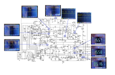
  1. As the Power Supply was inspected and voltage tests were at norms; +5.15vdc, +/-15.58vdc
  2. Plugged in all connectors (confirmed orientations)
  3. Inserted Digital, Analog, and Serial PCBs
  4. Checked and powered on
  5. Front panel lit all lights, then off, carriage shuttle centered, then printer error lit
  6. Within 1-2 seconds smoke emerged, and I powered off

Post smoke-test Inspection:
  1. Pulling and inspecting ALL PCBs, the Digital board showed the issue; L1 & L2, 2 100uH inductors fried!
  2. As re-inspection of the Power Supply showed it still functions and provides proper power.
  3. I am assuming because of age and the added load of other boards resulted in over heating of the inductors.
  4. Although the Power Supply PCB looks and measures OK, the L1 Transformer looks ugly; like it will fall apart any time soon…I might just outright assume it is bad too, but need to find a proper replacement
I can’t find clear specs for the L1 Transformer to know an equivalent to replace. Regardless, it does seem to provided (with other circuitry) the +5vdc & +/-15vdc out that is needed

PCB Power Supply L1 Transformer is labeled EIA3948109 (14631) - 92031B 1&2 for +15vdc, 3&4 for -15vdc, and 6&7 for +5vdc

Inductors L1 & L2 100uH on Digital PCB I can find/replace

Also, any other thoughts on possible causes?

Any more assistance or guidance on the above is appreciated
 
Last edited:
I can't find any documentation online for the LQP02 (schematics, etc). If you have hardcopies please scan them so they can be added to bitsavers.
I found schematics in the LQP02 tech manual on manx.

It sounds like there is a short on the digital board which causes L1/L2 to burn out. A likely failure point is electrolytic capacitors which can degrade over time. Visually inspect them and test/replace any that are swollen or leaking. It appears L1/L2 go to C44/C45 and then to U20 on page 4. That is where I would start looking.

CW
 
Last edited:
CW, Thanks for your response....

Yes...I already have that document. Looks like you been looking too....For others, refer to the following pages for this thread.
  • pg131 Digital board see grid F10 & F11 for L1,L2,C44,C45
  • pg135 Digital schematic Inductors L1 & L2
No Electrolytics, however a few Polypropylene Polarized caps at C44, C45, C6, and C16.....Although in situ, would still suspect at least C44 & C45; both 15uF, but have no resistance (OL)

Will take a look at U20 on page 4? Please confirm...Will trace too. On board is at grid C11 is U20; schematic 137; LM339=U20...Anyway, will look further...

As I am also concerned of load and overheating, I am looking at the following, transformer L1.....
  • 151 Power Supply Board L1
  • 153 Power Supply Schematic L1
Power Supply, board still good, but L1 is a little sketchy in the long run

Fried Inductors..
20240317_090410.jpg
 
Last edited:
Catching up and clarifications

Recap
After inspection and restore of LQP02, I decided to power up. Received some positive response and then components started to fail on the digital board. Some suspect went to age of components and power supply suppling service. Post inspection, looked at all boards for issues or potential failing components

Clarification
Power Supply PCB component L1 is not a Transformer, but an iron core Inductor. Visually, looked like a transformer and the "L1" should have been a clue; Ooops! Regardless, no specs
on the EIA3948109 inductor found and no response from manufacture (specs lost to time). Schematic is the only clue to use and it services +5vdc and +/-15vdc

Some progress
Post failure and detail inspection, I replaced components on Digital board, including L1/L2 Inductors (fried above) as well as 3 capacitors C44, C45, C6. Visual and probed inspection only revealed these components to be faulty or below tolerance/expectations.

Power Supply: Looking back at the Power Supply and inspection revealed no known or faulty components however still have two areas of concern:
  1. L1 (the iron core inductor) does not seem to be faulty but look like its melting over time.... (Concern only)
  2. On Test Points (TP3, TP4, TP5) there is a rising spike that does not look natural. I would like to understand this better and perhaps inspect and replace components that may be causing this anomaly. As source for all three TPs is Transformer T3 and the Inductor L2 is right before all three, then perhaps L2 might be a concern. After L2, there are two diodes VR2/VR3 that might be breaking down (before TP3 & TP4), but still the same spike is seen in TP5 without a preceding diode. (ergo...T3 and L2 to be examined)
    • TP3&TP4 - Cycles about every 50.5uS with a 10uS pulse at 40vdc. The rising spike hits about 70vdc before dropping to 30vdc and leveling to 40vdc
    • TP5 - Cycles about every 30uS with a 10uS pulse at 20vdc. The rising spike hits about 35vdc before dropping to 25vdc and leveling to 20vdc
All else on the Power Supply looks good and produces correct voltages without load. Illustration of the readings in the attached image

Any thoughts, tips pointers appreciated. Perhaps over observing nature state which is smoothed out by subsequent circuitry?
 

Attachments

  • Test Points 240321.png
    Test Points 240321.png
    1.6 MB · Views: 10
Back
Top