• Please review our updated Terms and Rules here

Macintosh IIsi Power Issues (Already recapped)

bretwashere

Member
Joined
Feb 2, 2023
Messages
13
Hello,

I have a Macintosh IIsi, which up until recently was working completely fine. It does not power on, and I don’t hear any signs of life coming from the power supply. The computer has already undergone maintenance on the motherboard as far as a full recap on the motherboard, and I personally just recapped the power supply.

So after quadruple checking my work, the power supply recap definitely seems like a success. I do have a few questions for further troubleshooting:

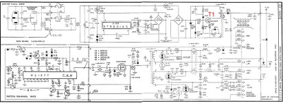
1) There is a relay inside of the Sony APS-06 power supply. Upon switching the computer on with the power button, should this relay engage? I do not hear or see any activity with this relay upon pushing power. I’ll include an image at the bottom of this post to show the relay I’m speaking about.

2) Is there a way to check system power and power rails using the SCSI port (The DB-25 or the internal 50 pen cable)? If so, can anyone please provide me with steps to perform this?

3) I’m sort of new to the electrical engineering aspect of my life. With that being said, what would be everyone’s next step for troubleshooting? I have replaced the 3.6 V battery, I have completely disassembled and reassembled the system (cleaning everything in the process), try different power cables, reset the RAM, removed the PDS to NuBus adapter. I do own oscilloscope, but I haven’t have any experience with it. Does anyone have a guide for how to test the power supplies rails directly, or information regarding how to use oscilloscope to troubleshoot a 68K Mac?

Any help to further troubleshoot this issue would be appreciated.

IMG_1141.jpeg

I also wanted to add that I did test continuity of the pins connected to the power button. They work as expected.
 
Last edited:
A little update: I spent the rest of the evening looking at a schematic of the power button to rule out the power button. I traced the power button continuity correctly to R148, and its continuity is correct on the 68HC05 chip, pin 25. So I highly doubt it’s the power button.
 
The protocols for diagnosing and repairing switch mode power supplies (SMPS) are generally all the same.

You can divide it very roughly into 4 basic things:

1) study of the particular supply's schematic and understand the theoretical operation of the supply.

2) Safety issues.

3) un-powered tests and measurements on components in circuit.

4) tests and measurements on the supply with line power applied, typically with the scope.

Many of the components, resistors, fusible resistors & fuses & diodes can be basically checked in circuit. As can in circuit testing be done in many cases on electrolytic capacitors with an ESR meter.

The output devices can sometimes be checked in circuit, but before jumping to conclusions, if the terminals appear shorted, be aware that with transformers driving BJT base-emitter junctions, and collector (or drain loads) you can get a reading that looks like a short in the device when it is not. Power mosfets and BJT's out of circuit are very easy to test with a bench power supply and a simple load.

In any case, once the un-powered tests are exhausted, and often this can be the case, a powered test is required. This means examining the drive waveforms to the power output device and the collector or drain load waveforms.

On the line side of the power supply there are safety issues, not only due to the line power there, but generally there is around 320V DC on the main filter capacitors.

In 115 V powered supplies this comes about because the configuration is a half wave voltage doubler. In 230V supplies it is full wave bridge. This sort of DC voltage level, originating from a low internal resistance source, is very nasty, and can be lethal, so avoid contact with it. It pays to leave the supply off for a while to allow these main filter capacitors to discharge before jumping in with passive tests on the components.

The result is though, that on the line side, not only are the electrical potentials in places high above ground, making a one handed shock a possibility, but it sabotages the connection of earthed instruments, like a scope. The "zero voltage reference level" for the line side of the psu, is the negative connection of the rectifiers & main filter capacitors. You can only connect your scope probe earth clip to that connection, if you power the supply via an isolating transformer. (one other method is to use a scope with isolated inputs like the Tek 222pS designed for scoping line powered circuits, but most workshops don't have one).

The voltages on the primary of the transformer can exceed 400 V, so it pays if scoping these, to use a x100 scope probe with a 1500V+ rating, to avoid damaging the input circuits on the scope or a typical x10 probe which are generally good to 400v. At least these x100 probes are cheap on ebay now.

Many SMP's use an IC of one type or another to drive the output power device/s (be they BJT's or mosfets), though sometimes it is done with discrete transistors. The general arrangement is that the supply output voltages are sampled, compared to a reference and fed back to control the duty cycle of the drive and thereby regulate the voltage. Often opto-couplers or transformers are involved in this feedback pathway to isolate the supply output from the line powered side. In addition, there are often over-voltage detection circuits. Errors from these can cut off the oscillator that drives the output devices and stop the supply that way.

The over-voltage detector circuits can get activated with the supply running out of the computer with no load, due to the transient power up voltage overshoots. So you will read it is important to check SMP's with an appropriate dummy load.

Also, most of these supplies have a starting circuit to get them going, then after starting the energy for that function is taken over by an output from the transformer. A failure in this circuit can render the supply non-operational too.

There is no escaping the fact that, while many SMPS can be repaired with re-capping and as a result of un-powered component checking finding a faulty resistor, capacitor or diode, a lot of the time this is good luck, and to be able to repair every supply requires the use of a scope and a good understanding of how the circuit operates. But you might "get lucky' on these simple tests. Still, my experience is , it is like the notion of walking into a Casino for the first time, putting a coin in a machine and hitting the jackpot. My view has always been to apply a logical method to get to the bottom of any fault and not rely on luck.

One of the early SMPS to be fitted to computers was the one in the 5155 computer. It kind of set a standard that many other designs followed. There is an article here on how it works. While it is not the same as your supply it will give you a kind of overview of "what goes on in an SMPS", as they are significantly more complicated than the iron cored transformer analog supply:

www.worldphaco.com/uploads/The_IBM_5155_POWER_SUPPLY.pdf

One way you can be helped on the forum is to post the schematic of the supply and mark on it what has been tested and how it was done. And that can give people ideas on what to test next.

As for the relay, I could tell you for sure if I could see the schematic. One issue though in all SMPS's that are over about 50 to 100W rated is the issue of turn on surge current. The line power that is delivered to your general purpose outlet in your home has a very low internal resistance, this is why you can draw 10 amps from it without the voltage sagging down significantly. Power Silicon rectifiers also have a low forward resistance, and the large filter capacitors in the PSU have a low ESR too. So when the line power is initially supplied there is a large surge current because the capacitors are starting at zero charge (zero volts on their terminals) and they get rapidly charged to around 300V (or lower values depending on the design). To mitigate this surge current (or inrush current as its sometimes called) the designers often put in a series power resistor. It would drop too much voltage and generate too much heat if left in circuit, when the supply was running, so in some designs they used the relay's contacts to short the resistor out, once the main filter capacitors were was charged. But the relay in your supply could have another application. However you will see a sub-circuit that does this on page 9 off the 5155 article in the link above. If your relay is for this purpose it should close shortly after power up.
 
Last edited:
That link is helpful and the OP should have provided it, plus there is more:

If the OP wants an A on an assignment and sends it in for marking, imagine the Professor marking the paper is sitting in his chair late at night with 30 papers to mark. There is a tray of stubbed out cigarettes beside him, and his glass of Jim Beam is already running out, and he is very tired too.

He starts to mark a new paper, but the writing is barely legible and what he can read is not entertaining either, now what sort of grade do you think that paper will get, regardless of its content ?

If information is presented to others, so that they can try to assess it, is should be presented in a way where it is easy to see.

That pdf for example shows the power supply split onto two pages and rotated 90 degrees.

One problem is, as you get older, the cervical spine degenerates and doesn't like rotating 90 degrees to read a document and you even have problems finding the option in the .pdf reader to tip it on its side.

Before I could even comment on this schematic, I had to paste both pages and join them together in a photo editor. This was the OP's job though, to "help people help him" by providing the information in an easy to read manner.

Looking at the circuit right away, there are two switch-mode circuits. The one based around T1 (which I labelled in red) is a self oscillating design which provides the starting voltage , it powers the driver IC for to the other switch-mode circuit. Though this self oscillating circuit is the "start up circuit" and the IC appears to need up to 17V to start (from the data sheet) after start up the 12V is sourced via the diode connecting the two +12V sources together, from the PWM regulated supply output.

The relay, in this case, does nothing special except to turn the power on the the auxiliary line IEC connector, which it will only do if the -12V rail from the IC controlled second switch-mode (PWM) circuit is working. Since that relay is not working, we can already deduce that the IC driven PWM circuit is not likely working.

So obviously the first check is to see if the self oscillating stage is working and check for the presence of the +12V supply there and +5V source derived from that with the zener shunt regulator, arriving at the vertical sub board with the M51977 PWM driver IC on it. This 5V source de-activates the PWM IC on its pin 7 and the switching transistor there (45 on the diagram), when driven , activates the IC by grounding pin 7. The +12V from the self oscillating circuit initially powers the IC too.

In this particular circuit, because of the isolation afforded by the transformers; T101 T102 and T104, you can connect an ordinary scope's ground clip to the common on the PWM sub board and check for 100kHz drive pulses on the IC's pin 2.

One other thing that helps is to look up the data sheet on the PWM IC, this one is the 20 pin version:


Attachments

  • PSU.jpg
    PSU.jpg
    328.5 KB · Views: 16
Last edited:
Hi everyone. Thank you for the replies. I haven’t had time this week yet to review everything, but I will do that soon.
 
@Hugo Holden I am going to start troubleshooting an Apple II Power Supply (Astec AA11040-B, 120 volt configuration) which has been recapped. The troubleshooting I've done so far is to measure the output voltage of DB1 which measures somewhere above 300 volts DC (I can't recall the exact measurement as it's been a few months since I worked on it).

I wanted to start scoping the supply (very interested in the signal at the base of Q2). In preparation I thought it wise to purchase an inexpensive battery-operated handheld scope (OWON HDS242) in order to avoid any potential ground loop issues with my bench scope. The maximum DC / AC voltage for the oscilloscope is 400 volts peak-peak, I assume this would be using the 10x attenuation of the supplied probe. I believe this should be sufficient but was thinking of purchasing a 100x probe just in case. Do you think the standard probe at 10x attenuation would be sufficient for troubleshooting this supply?

I have some knowledge of analog circuitry but it's been a while since I studied it in college. I am much better at digital than I am analog.
In this case you probably would be ok with a x10 probe and a battery operated scope, but it might cause some probe damage as the voltage transients can go over 400v pp, probably not by an awful lot. But a x100 probe would be better. At least if you do use a 400v pp x10 probe, make sure the scope is set on 50v/cm to avoid input damage to the scope.
 
@Hugo Holden question for you, I recapped a IIsi Power Supply, and upon testing it the 2SK10402A MOSFET (as circled below) self destructed.

I suspect there's something wrong with the vertical sub-board, any ideas? I want to measure the +12V and +5V supplies, and check for 100kHz drive pulses on the IC's pin 2, however access to the pins is quite tricky and I have to make sure it's safe to work around the board due to the nasty AC & DC voltages you mention.

1731549046417.png
 
It looks from the design that it is ok to check the sub board, as it runs from the secondary side of the power supplies and shares its common with those. It gets its isolation from the line power side from the coupling transformer T102 that drives the gate of the blown mosfet and from the feedback transformer T103.

The big question is why did the mosfet fail? I'll list a few scenarios:

1) If it is not properly enhanced (the gate drive voltage not high enough, it then dissipates a lot of power because the drain to source resistance is too high. So the output of the PWM IC should be checked that its a solid drive voltage . Also, if the coupling capacitors in either side of T102 lost capacity that could do it, sometimes certain metalized plastic film types do this, similar to the X2 types. In one extremely odd case I saw an example of the two ferrite halves that make the doupling transformer part a little when the glue fractured, lowering the inductance and differentiating the drive wave, but that is rare scenario.

2) Mosfets don't like their gate-source voltage exceeded. That is the idea of the zener in the gate circuit, to prevent that, so worth checking it.

3) high voltage transients or voltage spikes, exceeding the mosfet's drain voltage rating. This also leads to catastrophic failure.

You will notice that on the collector circuit, there is a diode feeding a capacitor with a bleeder resistor across it , but the positive voltage generated at the cathode of the diode and resistor "connects nowhere". This circuit idea is very old, it had is origins way back in the 1960's in DC/DC converters with Germanium power transistors, that were limited in the collector voltages they could handle. This circuit was often applied to the collector of the transistors. It is a "dynamic voltage tracking snubber". What happens is the capacitor is charged to the peak voltage of the rectangular switching wave or close to that. If there is a high voltage transient on the leading edge of the wave the capacitor tends to snub it off. The bleeder resistor is required to discharge the capacitor in a reasonable time frame, but that is much longer than the times between the short transients. If there was no bleeder resistor, the capacitor simply would ultimately charge to the amplitude of the peak of the voltage spike and then the snubber circuit would not work. So, for example, if that diode D103 went open, or the resistor R103 went open or the capacitor C103 lost uF value, the mosfet would likely be destroyed by the un-snubbed high voltage transients on its drain circuit. Clearly those parts need checking.

4) it is possible in some cases (though its not ideal) if the secondary side of the switching supply transformer T101, was not connected to its loads, the primary voltage transient increase could destroy the mosfet, but usually most designers allow for a zero load scenario at least not damaging anything.

5) Sometimes these switching parts in SMPS supplies and H output stages of TV's just spontaneously fail and nobody knows why, except they are usually parts under high voltage and or high current stressors. Many TV's and VDU's would turn up at repair shops, and parts like this found to have failed. However, when there was an underlying cause often not detected by the technician (such as a defective snubber component) usually what happened is that the set bounced back with the same fault within a week, with the customer saying they we happily drinking their Beer and watching their favorite sports game and the screen went black again. So it does pay to check out as much as possible.

Unfortunately something did happen to foul up the most logical plans of Mice & Men in trying to determine the real cause of these sorts of failures. Fake transistors. In this sort of application repeat failures will readily occur, even without faulty parts elsewhere in the circuit, if the transistor is a clone or fake, so when you replace it try as hard as you can to acquire a genuine part.
 
Back
Top