This post details a simple modification that I made to the video generation circuitry of my PET-2001 clone to make all modes of video RAM access 100% snow free, but the basics are something that could be easily done to an original 2001 if the video SRAM and character generator ROM chips are upgraded to modern devices having modern access times.
This RAM/ROM upgrade/substitution could be achieved with SMD adaptor boards that simply plug into sockets replacing the two 6550 (200nS) 1Kx4-bit SRAM chips and the one 6540 (300nS) 1KB ROM.
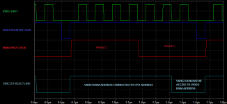
Here is a timing diagram specific to my clone:

All the modification does is generates an alternative drive signal for the select line going to the three 74HC157 multiplexer ICs in the video generator. This select line, when asserted, grants the CPU access to the address lines of the video RAM and it was originally connected to the video RAM address decoder.
6502 read and writes are initiated at the end of the Phase 2 period (the falling edge of the PHI2 master clock for the WDC65C02 in my clone). The shift register which serially shifts out the video signal is loaded with one row of character pixel data every 1000nS, at the end of the Phase 1 part of the clock period. 6502 address set-up starts at the beginning of Phase 1 and this is why snow is generated during video RAM access during active screen time - the CPU has gained control of the video RAM address lines before the shift register is loaded.
With fast enough RAM & ROM, however, video RAM address access need not occur this early in the 6502s clock period and we can avoid interfering with the shift register loading altogether.
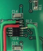
Fortuitously, I had one spare 2-input NAND gate on my video generator board:

I lifted the input pins of this gate, which were originally grounded, and wired them to appropriate outputs of the video generator row counter circuitry to produce the waveform labeled "74HC157 SELECT LINE" on the timing diagram posted above. This signal goes low for the 250nS second half of the Phase 1 period.
The select line to the 74HC157 video RAM address MUX ICs was disconnected from the video RAM address decoder and rewired to this new control signal.
This has significantly altered the way the video RAM address lines are connected to the CPU address bus. The video generator circuitry now accesses the video RAM on an interleaved basis with the 6502 and the 6502 can no longer interfere with shift register loads.
The video generator gets access to the video RAM ~250nS prior to the start of phase 2. This is plenty (eons actually) of set-up time for the modern RAM and ROM used in my video generator.
Note that the original PET used 200nS RAM and a 300nS ROM. To the sum of those you have to add the propagation delay of the 74**157 address MUX and the data set-up time for the shift-register. Definitely don't try this on an original machine without a video RAM and ROM upgrade!
Incidentally, this interleaving approach to video RAM access is basically how more modern 6502 computers such as the VIC-20 and the C64 handled their video generation - "snow" free.
I'm kinda slapping myself on the head for not designing my modern PET-clone to work this way to start with.
This RAM/ROM upgrade/substitution could be achieved with SMD adaptor boards that simply plug into sockets replacing the two 6550 (200nS) 1Kx4-bit SRAM chips and the one 6540 (300nS) 1KB ROM.
Here is a timing diagram specific to my clone:

All the modification does is generates an alternative drive signal for the select line going to the three 74HC157 multiplexer ICs in the video generator. This select line, when asserted, grants the CPU access to the address lines of the video RAM and it was originally connected to the video RAM address decoder.
6502 read and writes are initiated at the end of the Phase 2 period (the falling edge of the PHI2 master clock for the WDC65C02 in my clone). The shift register which serially shifts out the video signal is loaded with one row of character pixel data every 1000nS, at the end of the Phase 1 part of the clock period. 6502 address set-up starts at the beginning of Phase 1 and this is why snow is generated during video RAM access during active screen time - the CPU has gained control of the video RAM address lines before the shift register is loaded.
With fast enough RAM & ROM, however, video RAM address access need not occur this early in the 6502s clock period and we can avoid interfering with the shift register loading altogether.
Fortuitously, I had one spare 2-input NAND gate on my video generator board:

I lifted the input pins of this gate, which were originally grounded, and wired them to appropriate outputs of the video generator row counter circuitry to produce the waveform labeled "74HC157 SELECT LINE" on the timing diagram posted above. This signal goes low for the 250nS second half of the Phase 1 period.
The select line to the 74HC157 video RAM address MUX ICs was disconnected from the video RAM address decoder and rewired to this new control signal.
This has significantly altered the way the video RAM address lines are connected to the CPU address bus. The video generator circuitry now accesses the video RAM on an interleaved basis with the 6502 and the 6502 can no longer interfere with shift register loads.
The video generator gets access to the video RAM ~250nS prior to the start of phase 2. This is plenty (eons actually) of set-up time for the modern RAM and ROM used in my video generator.
Note that the original PET used 200nS RAM and a 300nS ROM. To the sum of those you have to add the propagation delay of the 74**157 address MUX and the data set-up time for the shift-register. Definitely don't try this on an original machine without a video RAM and ROM upgrade!
Incidentally, this interleaving approach to video RAM access is basically how more modern 6502 computers such as the VIC-20 and the C64 handled their video generation - "snow" free.
I'm kinda slapping myself on the head for not designing my modern PET-clone to work this way to start with.
Last edited:
