• Please review our updated Terms and Rules here

MFM decoder for RL02 = up and running but sector/header format unclear and ...

PDP11GY

Experienced Member
Joined
Jun 20, 2009
Messages
145
Location
Munich/Germany
.... a spare RLV-11/12 still needed.

In view of the very sad events in Japan, everything gets relative....

Hello,
concerning my post October 12th, 2010, first of all, the MFM decoder for the RL02 with clock and data recovery is ready, up and running and is available via my homepage, chapter 1.7. The bad thing is, that I was running in another problem: The RL02 cartridges were factory formated and the Servo/Header format was strictly company confidential . In the Servo/Header section of the RL02 disk cartridge format appears sometimes a 0.125uS or 0.625uS MFM signal ( 0.250uS, 0.325uS, 0.500uS is normal ) which will confuse my MFM decoders. I have implemented a work-around ( see homepage ) but I need a exactly description of the servo/header format of the RL02 cartridges. Any idea where I could get the upgrade info ?
My second question: I could solve the problem as described in my last post by replacing the DC005 and the DC004 Q-Bus chips. Unfortunately, an error has happened to me when soldering and now I have contact problems and I amstill looking for a spare RLV-11/12.
Every Info and/or indications is welcome

Regards, Reinhard
 
For those who may be interested, this article is related to Reinhard's first request.

I may have something on this... I will look. I know DEC kept the ability to create RL media
pretty confidential.
 
Would be very helpful if you can collect the info. Otherwise , reading the contens from the MFM data sequencer EPROM ( 2708) may be also helpful and maybe a listing about the contens is available anywhere ? Many thank in advance and best regards.
 
Reinhard, please look at the RL02techDesc ,document section 2.2 [pdf page 39]

This document outlines the Servo information to a great detail. The "Count Rom" contents, and Decoder will also be required to completely understand the mechanism. [See pdf page 113, 115 table 5-2, 116 5-4]


I'm not really sure why you need this data, because it is my understanding that this info is processed on the drive itself, and not the QBUS / UNIBUS control. It would only be needed if you were planning to fabricate or initialize RL "cartridges".

Am I incorrect?

Anyway, I think this document has what you "seek". :cool:
 
Last edited:
Hello und many thanks providing this info. I did already collect the infos ( bitsaver.org) and also the RL02 and RLV-11 engineering drawings. Good point from you : " I'm not really sure why you need this data". I agree , especially the servo information is necessary for the drive only. But, the sector header is located betwenn the PR1 and PD1 servo information. Consequently, my RL02 simulator must provide the illusion to the RLV-11 controller, that a RL "cartridges" is available with valid header structure and header-CRC. Regards, Reinhard
 
Thank you Reinhard,

In the same document, please see Figure 1-10 pdf page 33, 36, 38 and associated text.

The only thing that remains unclear to me is the precise CRC algorithm employed by the RL Controller. [I find a single IC on the RL schematic processes this so it can be understood from there]

I must assume you have already solved this CRC question. (?) [UPDATE: The chip is a Fairchild 9401 / 74F401 and is wired for CRC16]

UPDATE2:
On review, I must again point out that the header and data details are implemented in the RL controller, and a purist "Drive emulation" would not limit changes in this area. In fact there are notes in the documentation about this very fact and DEC provided low level functions to perform I/O without this format being imposed.
Are there any other aspects I can help with?
 
Last edited:
Hello and many thanks for your efforts
perhaps we have a small communication problem ?
The CRC algorithm is not relevant for me in this project , because this will be executed inside the RLV-11/12 controller based on a CRC genarater chip 9401 ( E3 ).
Perhaps I can littly hereby explain my problem better:
I can already read and decode the MFM data from one trock/sector.
The problem happens in the header area:
|----PR1(3word)---|---HEADER(3words)---|---PD1(1word)|---PR2(3word)---|--DATA.....
the RL02 runs with a 4.1MHz transfer clock. Through this, it produces 3 different MFM
periods, 0.250uS, 0.325uS, 0.500uS, But in the HEADER area, sometimes a 0.125uS or 0.625uS MFM signal appears.... and that is my problem.
right now, for me it looks like a alignment feature. because the HEADER area is
allways 3 word long, but the contents is different dependend from the sector number, which will result, that the length of the MFM signals must be re-aligned ? Example: A) 00000 would be 1us, B) 00101 would be 1.250uS. Case A) a re-aligment is necessary with additional 0.250 uS.That's my assumtion . Anyway, I can't continue to work because I have definitely destroyed my RLV-12 controller during a try to fix the contact problems via re-soldering. Too bad...
 
Hello and many thanks for your efforts
perhaps we have a small communication problem ?
Yes, I agree... thank you.
The CRC algorithm is not relevant for me in this project , because this will be executed inside the RLV-11/12 controller based on a CRC genarater chip 9401 ( E3 ).
Again, I agree, it should not be needed for you to decode this unless you want to do a CRC verification yourself as a diagnostic. My misunderstanding is that I thought you were looking for a complete understanding of the PR1-through-PO2 block.
Perhaps I can littly hereby explain my problem better:
I can already read and decode the MFM data from one trock/sector.
The problem happens in the header area:
|----PR1(3word)---|---HEADER(3words)---|---PD1(1word)|---PR2(3word)---|--DATA.....
the RL02 runs with a 4.1MHz transfer clock. Through this, it produces 3 different MFM
periods, 0.250uS, 0.325uS, 0.500uS, But in the HEADER area, sometimes a 0.125uS or 0.625uS MFM signal appears.... and that is my problem.
right now, for me it looks like a alignment feature. because the HEADER area is
allways 3 word long, but the contents is different dependend from the sector number, which will result, that the length of the MFM signals must be re-aligned ? Example: A) 00000 would be 1us, B) 00101 would be 1.250uS. Case A) a re-aligment is necessary with additional 0.250 uS.That's my assumtion .

Ok, I think I understand.
There is nothing in the header that should produce edges at 125ns spacing. The shortest time interval between edges on the MFM should be 250ns, not 125ns. The other spacings should be 375ns [250+125] or 500ns. Likewise, edge spacings of 625ns are completely incorrect if they appear between the PReamble and POstables. This is what you see as wrong, and I agree.
I find it more than a coincidence that the 90 degree MFM modulation phase-change equals 125ns.

I've looked closely at your homepage. I admire your tenacity. Seeing there, what you are doing, give me ideas to ask some questions. Pardon me, but I'm still catching up to you.


  • Did you use the SECTOR PULSE to remove [gate off] the "Servo burst data" from the drive's MFM stream? I could see it might confuse the DPLL and MFM decoders.

  • How are you sensing the presence of the 125ns you are detecting? Are you able to see it through a scope? In other words - are you convinced it is REAL? and not a digital artifact?

Anyway, I can't continue to work because I have definitely destroyed my RLV-12 controller during a try to fix the contact problems via re-soldering. Too bad...
I'd offer to try to fix it for you, but I see you're pretty far away. I hope you'll have luck finding another.

Perhaps I could make a suggestion. If you go ahead and program your development system to include the MFM Encoder, you could continue your work without the RLV12 until such time as it is repaired. By "Looping back" MFM signals, you could verify your design, against your own understanding and the documentation [which could have unmentioned secrets]

If you can make this work, you would be in a position to issue read commands to the RL02 yourself, further verifying your designs.
This would be very handy for your intended audience too. For example - a hobbyist wants to transfer his RL02 media contents to his PC, because he has no PDP-11 and want to run SIMH or E11. He is able to do this because he uses your device to "CLONE" the RL disks, to a FLASH CARD which is PC readable. [through a program]

No PDP-11 System Required.

Also, the hobbyist who has a PDP-11 [or other system] but receives his RL02 content over the internet and wants to return it to a real RL02 media, could use the reverse process through your device to do so, without using the system CPU.
Perhaps you've already thought of all this. Forgive me, I find your project exciting.
 
Last edited:
Question about your design...

Question about your design...

I've been digging into your MFM-Phase-Timing.jpg and MFM_Decoder.jpg diagrams and comparing them with the patent, and with diagrams in the DEC documentation.

I'm trying to understand the operation of your decoder, and it's generation and use of a 4.166Mhz clock, synchronized with MFM data.

Could you help me understand your design choice to use an MFM clock of 4.166Mhz rather than 8.333Mhz?

In looking at DEC's design, they use a 4x bit clocking scheme to convert the NRZ bit stream into MFM. This made the modulation of +/-90 degrees easy to do.
DEC_NRZ-MFM.jpg

...This diagram is from Page 46 of RL02techDescr.pdf


Wouldn't using a similar scheme in the MFM decoder make the DPLL work better by synchronizing the 4x clock to every input MFM transition?


Last edited:
Hello and many thanks for all the notes.
Concerning my design and the 4.166Mhz clock: I did try to reconstruct the 4.1 Mhz. On a FPGA, like a CYCLONII a PLL is available, but you can only rebuilt a clock running at 4.076087 Mhz. I decided to use a 12:1 divider which brings me to 4.1666 Mhz. The advantage of this method is that it can be also implemented on a MAXII CPLD because on a CPLD no PLL is available. Maybe you have already looked on my homepage chapter 1.7 C) where you will find at the end links to
the circuit diagrams. they exported in JPG - format but I can provide the entire working folder based on Altera Quartus software , including programmes for the ARM CPU via E-Mail.
Some generally infos: I am able to:
- read the drive status command. - send the drive status. - rebuilt the sector puls. - collect the data during a write cycle ( write gate ) During the read operation, the 4.1Mhz system clock is not available and I decided to implement a MFM decoder with clock and data recovery. The reason to do this was to generate a formated SD card which includes all servo/header infos. The same way like DEC has done it with the factory formated cartridges. If this will work fine, I will implement a MFM-encoder. This should be possible more easily because the 4.1 system clock is available and can be doubled to the necessary 8.2Mhz. Your question to use an MFM clock of 4.166Mhz rather than 8.333Mhz... now , because the transfer clock rate is 4.1Mhz and the data on the cartridge is based on this frequency. I agree , a 8.2Mhz clock is necessary designing the MFM encoder.
Concerning your post before: generelly, I am still in the learning phase working with FPGA design and I know, I am thinking still too much asynchronously and I also know, there is a lot of improvement possible in my current design. Also, I am learnig the Verilog language to be able to improve my design much more. My current available MFM decoder with clock recovery works fine with the exception that the servo/header area makes problems. Your question "How are you sensing the presence of the 125ns" The MFM data consists of 3 diffent periods and I have implemented a circuit which will match if no valid MFM is detected. This circuit generates a puls and can be analyzed via logig analyser. Your question: "Did you use the SECTOR PULSE to remove [gate off] the "Servo burst data" ... yes I did it. I don't know why it schould confuse the DPLL. What is the background of your assumption ? Please can you explain it to me? I figured out, that the MFM data will start after about 9.6uS if sector-pulse = High.
Anyway, thank you very much for all your infos.
To work continue, I have to fix the problem with my RLV-12 controller first.
You are right, .... you are too far away , but I appreciate all the help !
 
Last edited:
Some more infos

Some more infos

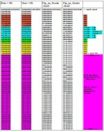
Enclosed , please find a analysis of the RL02 servo/header data problem.
 

Attachments

  • MFM_header_problem.jpg
    MFM_header_problem.jpg
    100.8 KB · Views: 1
Thank you for your previous answers, and your patience.

For my new questions, I will restrict myself only to the First
"OK" column of the previous attachment.

1) Am I correct to interpret each line of this demodulated data is read RIGHT-to-LEFT?
The PReamble is supposedly 47 logical "0" followed by a "1" [48 bits total]

The first
"OK" column of data shows PR2 as:
00000000
00000000
00000000
00000000
00000000
10000000
Is this the sequense of these bits?
76543210
FEDCBA98
...
2) It concerns me greatly that PR1 PR2 are not the same, even though they should be.

3) All POstambles should be 16 "0" bits, and they are not.

4) Can I assume this data is taken only during the SECTOR PULSE?

The HEADER should be 112 bits long.

All this makes me want to question the HEADER / DATA alignment in the frame, or the MFM Demodulator output.​
 
Hello,

the output schows the bits with the LSB on the right site.
1) In case of PR2:
00000000
00000000
00000000
00000000
00000000
10000000
|------------------>bit 47 ( and 48 bits total )

2) You are right, the PR1 is not the same as PR2, but should be
3) Yes, should be 16 "0" , but is not.

4) The header field contains three words ( 6 byte ) of 16 bits each.

I did implemt the alignmet for the data as follow: In the middle of PR2 , the
date will be forced to set to "0". Than , I wait for the PR2 sync bit and allign
the data to 16bit boundary.
This works fine for the data and I always can decode the data faultless, for example
a text file where I can see the output always correct.
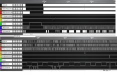
Enclosed find the timing via jpg - file.

Regards , Reinhard
1.jpg
 
This discussion is very helpful to me - Thank You.

Reinhard, at this point I am still questioning everything. The data you've gathered don't look like what I expected. [Perhaps just a little]

I need to decide what I can do about that.
As you are aware, I'm planing to do a similar device to convert MFM ST-506 style data to a flash drive, so I thought helping you - would also help me.

Now it seems, that in order to help you, the only thing I can do is try to re-create your system, here. That way I can verify what you are seeing or perhaps spot the problem.
I am not prepared to power up my PDP-11s after so long, without extensively checking power supplies and other large components first. This will take time, and I don't think it will be speedy enough to be of assistance to you. It is also not the NEXT thing I should be doing for my own project, although it will be needed eventually.

Perhaps it would be best to get behind me, before I proceed too far with other work. I am not sure.


-------------------

Some other thoughts while I am pondering what I can do...

1) I realize with your RLV12 inoperative, you cannot do it now, but did your RL02 work as a system disk without errors prior to this?

  • For example, was your PDP-11 able to boot from it and run programs?

  • In other words - Do we Know for Certain that the Drive, Disk and Cabling are sound and operate without error?

  • Could you take the Drive, Disk and Cable to another system temporarily, to re-check them?
2) You have constructed an interface to connect the RL02 cable to your development system.

  • Is it possible to verify that this is treating signals, especially MFM DATA, correctly so that your Decoder is being presented with good data?

  • Perhaps a comparator that looks at the logic levels before and after the "driver-cable-receiver" interface?
3) Once again, I am thinking you could try to check your decoder by "Simulation".

  • Make a device to output a "known good" STANDARD MFM signal. Feed this to your MFM Decoder as a test.

  • Perhaps one of the Development boards you no longer plan to use could do this?

  • You could choose to output a CLOCK signal from the SIMULATOR to eliminate the DPLL as a source of error at first. Later, you could disconnect the CLOCK and re-test against the same Simulated STANDARD, in "data only" mode.

  • Make "Flavors" of the STANDARD to stress the decoder. Ideally, One of these flavors should duplicate an RL02 sector as exactly as you can, based on the documentation.
[I think we have enough defined now from the documentation to be sure of this? ]
Are these thoughts helping you at all?
 
Last edited:
URGENT - Please Read

URGENT - Please Read

... My current available MFM decoder with clock recovery works fine with the exception that the servo/header area makes problems. ...

...Your question: "Did you use the SECTOR PULSE to remove [gate off] the "Servo burst data" ... yes I did it. I don't know why it schould confuse the DPLL. What is the background of your assumption ? Please can you explain it to me? ...

I found this answer, and it may cause you to re-think your DPLL implementation a little, in addition to the HDR / DATA read.

It is from the RL02techDescr.pdf [pdf page 54.]

Read Data (RD DATA)
This line transfers MFM encoded data from the drive read circuits to the controller. During the absence of any command and whenever a drive is selected and Drive Ready is asserted, Read Data appears on this line.

The drive senses the amplitude of the header preamble and sends Read Data over the Read Data line 2.5 +/-0.5 microsecond downstream from where the preamble actually starts.

For reading headers, the VFO loop is phaselocked with the arrival of Read Data after the end of the sector pulse.

For the data preamble, the VFO locks 32 read pulses after the header CRC to avoid transmitting erroneous sync pulses to the clock at the transition between the pre-recorded header and the data preamble. Detection of the preamble marker commences after the VFO has had time to phase lock.​
This would explain too, why you might have illegal timings and extra bits in the interval between PO1 and PR2.

In other words, whenever you are awaiting a PReamble, you need to be sure the PLL is already locked. Once it is, then wait for the occurrance of 00000001 at the MFM output to actually know you are at the end of the PReamble, and at the beginning of the HDR or DATA. [SYNC on "1" in essence]

This should go a long way to resolving your issues.
 
Last edited:
Hello and many thanks for this very importend information.
Seems to be, I was apparent in a loop of a thought-process and could not find the exit.
Your note is very important for me and explains, why I see illegal timings and extra bits in the interval between PR1 and PR2. With the help you provided, I see an exit now. This gives the indication to me, that I have to split my MFM decoder in two areas, the 1) Servo/header and the 2) data area. Part 2) is done and works, but part 1) may go very difficulty. What do you think about the following idea: Remove the EPROM 2708, E8 on a RLV11/M8013, read the contents and import the data in the FPGA world ? I think the secret is in this EPROM based on the flow chart info in the RLV-11 engineering drawings. I am thinking about this, because I got the message yesterday, that the computer museum in Munich could find RLV-11 ( M8012,M8013 ) boards.
Concerning your last post:
Generally, a question arises to me: Should I investigate more effort in the RL02 simulator or should I switch over to a MFM ST-506 style disk simulator, working together with you ? The realization would be much more simpler. I have an up and running DEC professional 350 and my special PDP11/23 with Q-BUS/CTI-Bus converter, also with an attached RD51 is available. The ST506 interface is running at 5Mhz and don't need the exotic 75107 and 75113 bus chips running with +/- 5 volt.
My environment: I have an up and running RL02 disk drive available, tested with XXDp and bootable RT-11 system , Macro-11, Fortran and Basic on it. 3 Cartriges are available, one is not useable. Reason: May be you can reminder about the problem with the magnetized RL02 heads which did result in a minified Servo/Header signal. This cartridge seems to be infected by this symptom. Reformat is not possible in the contrast to a ST-506 style disk.
My 2 development boards, connected to a MAXII and a CYCLONII as well my cable environment is working fine an I see no reason to verify it again. Concerning Simulation: From my point of view far too much overhead and investigation would be necessary.
Best regards, Reinhard
 
...This gives the indication to me, that I have to split my MFM decoder in two areas, the 1) Servo/header and the 2) data area. Part 2) is done and works, but part 1) may go very difficulty.

I suppose this would be one way to accomplish it, but I think you might consider a simpler approach.

The thing that appears missing from the design at this point is the notion of Byte "SYNC" on the decoded MFM data, as well as imposing a LOSS of SYNC at a known place in the end of the HEADER before the DATA Preamble.

It appears to me that you can add a single stage which waits for the "1" at the end of the PReamble(s), before outputting correctly framed data 8 bits at a time.

This should correctly "FRAME" the HEADER bits you've had so much trouble with.

The size of the HEADER needs to be to measured so that when the final bit of the CRC is received, you must intentionally "UN-SYNC" the stage for 32 bits. This provides a means of "skipping over" the intersession gap between the end of the HEADER and the beginning of the DATA".

What do you think about the following idea: Remove the EPROM 2708, E8 on a RLV11/M8013, read the contents and import the data in the FPGA world ? I think the secret is in this EPROM based on the flow chart info in the RLV-11 engineering drawings. I am thinking about this, because I got the message yesterday, that the computer museum in Munich could find RLV-11 ( M8012,M8013 ) boards.
Are you thinking you need to process the SERVO data to be able to read the header correctly?

I don't think you need to do this at all. Ignore the SERVO data entirely. By "Gating Off" the MFM data during the inter-SECTOR pulse, you are already accomplishing this.

The reason you have not gotten your headers read consistently is that you are not SYNCing on the end of the PReamble, so the bits are not being FRAMED correctly into 8 [or 16] bit words.

Concerning your last post:
Generally, a question arises to me: Should I investigate more effort in the RL02 simulator or should I switch over to a MFM ST-506 style disk simulator, working together with you ? The realization would be much more simpler. I have an up and running DEC professional 350 and my special PDP11/23 with Q-BUS/CTI-Bus converter, also with an attached RD51 is available. The ST506 interface is running at 5Mhz and don't need the exotic 75107 and 75113 bus chips running with +/- 5 volt.

I think you're hot on the RL02. If I were you, I would stay with this until you kick it's ass totally!

My environment: I have an up and running RL02 disk drive available, tested with XXDp and bootable RT-11 system , Macro-11, Fortran and Basic on it.

3 Cartriges are available, one is not usable. Reason: May be you can reminder about the problem with the magnetized RL02 heads which did result in a minified Servo/Header signal. This cartridge seems to be infected by this symptom. Reformat is not possible in the contrast to a ST-506 style disk.

Ok, this tells me that you know which cartridges to trust, and which not to. Unless you suspect something has changed there is no need to do my previous suggestion "1)".

My 2 development boards, connected to a MAXII and a CYCLONII as well my cable environment is working fine an I see no reason to verify it again.

If you are confident, then there is no need to do my previous suggestion "2)".

Concerning Simulation: From my point of view far too much overhead and investigation would be necessary...
You are the boss!

However, I might point out that your final device, emulating an RL drive well enough to fool a RLV1x controller and software system IS a SIMULATOR of sorts. It's just not taylored for your needs now.


One final observation:

In defense of my suggestions...

RL02 Cartridge FORMAT is written in at least 3 Separate "SESSIONS". This is the reason there are gaps between the SERVO, HEADER, and DATA portions of a SECTOR.


  • SERVO data is written as the first stage in bringing an RL disk to life. This can only be done by DEC at the factory because the RL drive does not have the ability to create this data, only to use it. Think what you like about the "Approach" of "SERVO in DATA", but it was a big advance for the time, and reduced the cost, complexity, and unreliability of disks in it's era.

  • Next, the disk is "FORMATTED" for the first time. The first HEADERs are written at the same time as the first DATA frames, but this is the only time they will be written together. Writing to both areas of the sector for the first time, the BAD sectors are discovered, and BAD BLOCK file can be created and recorded.
    It is worth noting that the BAD BLOCK file contains 5 redundant copies of bad sector data, to ensure that one of them will be readable. It also distinguishes the FACTORY discovered "bad areas" from the subsequent ones.

  • As soon as the DISK is USED to contain real data, that DATA is written down in yet another session.

This is why the HEADER must be separated from the DATA on read, - it was not written at the same time and therefore could not possibly be laid down with enough accuracy to prevent illegal timing intervals.

"Byte SYNCing" FRAMES with the PREAMBLEs solves the problem for both HEADER and DATA segments of the sector.
 
Last edited:
Hello,
concerning your note: "Are you thinking you need to process the SERVO data to be able to read the header correctly?" Some info: The source of the READ signal normaly is the RL02 disk drive. To be able to collect the MFM data within the READ signal, I have added an additional amplifier ( 75113 ) to watch and analyse all the date which normaly receives the RLV-12 controller. This meens, my MFM decoder runs effectively parallel to the decoder in the RLV-12 contoller. I used this trick because it is needful to implement the concept with a formated SD card. In my opinion, I have to rebuilt the Servo/header exacly, because the RLV12 controller works as designed and expects all the SERVO/Header infos. My conclusion concerning the development of the outstanding MFM encoder, I must fake the SERVO/HEADER signals, otherwise the RLV-12 controller will go confused. Do you agree?
 
Would it be easier to prototype with ST-506 so you didn't have to deal with the 4.1 clock or explicit data format?. You could concentrate on MFM encoding/decoding @ 5MHz and let the controller write a low level format to test with. Then once that works, move to 4.1 MHz and write a utility to 'low-level' format your SD cards. Just a suggestion :)
 
Hello,
concerning your note: "Are you thinking you need to process the SERVO data to be able to read the header correctly?" Some info: The source of the READ signal normaly is the RL02 disk drive. To be able to collect the MFM data within the READ signal, I have added an additional amplifier ( 75113 ) to watch and analyse all the date which normaly receives the RLV-12 controller. This meens, my MFM decoder runs effectively parallel to the decoder in the RLV-12 contoller. I used this trick because it is needful to implement the concept with a formated SD card. In my opinion, I have to rebuilt the Servo/header exacly, because the RLV12 controller works as designed and expects all the SERVO/Header infos. My conclusion concerning the development of the outstanding MFM encoder, I must fake the SERVO/HEADER signals, otherwise the RLV-12 controller will go confused. Do you agree?
No, am afraid I do not agree.

I do not find that the SERVO data is processed in the RLV at all. It is processed in the drive itself, to allow the heads to center on the correct track, and to fine tune the velocity - after which it is ignored unless the alignment changes or the velocity drifts. [Neither of which actions are taken or noticed by the RLV] If the drive were unable to process the servo data, it would never send a READY to the RLV controller at all.

I will look for direct evidence of this in the documentation if you wish, but I am certain.

I am not certain, however, what this has to do regarding the SD card part of the design? This we have not discussed.

I can understand that your device was initially constructed to watch the data as it was read by the RLV12. [a very good approach for the beginning] I had assumed this was to quickly and easily have good data to watch - without having to yet send the commands to the Drive yourself to get the data, and to make use of the RLV checking that the data is good. [valid CRC, no seek error]

If I look at your previous document "MFM_header_problem.jpg", I believe I can separate valid header and data from your capture by re-aligning the bits to their correct position using the expected PReambles, as the quoted excerpt from RL02TechDesct.pdf [pdf Page 54] suggests. The thing that is wrong with these data are that the bit framing, in words is incorrect, a fact which we have now explained and understood.

Finally, although I think it is a waste of your time and will not benefit you, the contents of the "Count ROM" are already published in the manual [pdf page 115&116], as I previously pointed out. You do not need to de-solder anything to know it's contents, unless you do not believe the documentation.

I do not comprehend why you still include the SERVO information in your plans at all. Can you explain this to me? I must be missing something.

You have done a great deal of work here. I think you are almost done being able to capture and interpret the sector contents. I can appreciate how frustrating it has been.

I am not sure what else I can say to help you.

Best Regards, as always.
 
Back
Top