• Please review our updated Terms and Rules here

Microkit 8/16

>>> Nice work!

Cheers :).

>>> I regret I don't have a logic analyzer nor a 1702 burner.

Never mind. Put it on your Christmas list for Santa...

>>> I guess there's no way to 'trick's the Microkit into displaying the missing data?

That is what I will work on tonight when I go for my evening walk!

I have found in the manual where it states that there is an automatic bootstrap load on power-up, so there maybe something wrong with your power on restart 555 that we may need to look at.

On power-up, the ENABLED light should light on the keyboard when the bootstrap starts to execute.

Dave
 
Well changing out a 555 is no big deal, if that's what you're thinking.

I have a bad feeling the only way this thing operates for us is if we find the original software. Can't even really make our own, I would assume the proprietary reading and recording format used precludes that. I have been emailing around to Genrad/successors trying to see if anyone might have anything. Highly doubtful. I really wonder how many of these were made given the low serial. Surviving materials might be very hard to come by.
 
>>> Well changing out a 555 is no big deal, if that's what you're thinking.

It may not be the 555 of course. That is not our pressing problem for the moment though...

I have found out a LOAD of information this afternoon... I have been looking at the schematics for the other cards (16K static RAM card and the 80 column VDU) and I think I have worked out how they work - and applied that to what I suspect. Interestingly, I can see how the BOOTSTRAP PROM now works a bit more (i.e. the BOOT code and the hardware I have gleaned seem to match!).

Each 8K RAM card has a write protect register of 8 bits. This write protects or write enables a block of 1K of RAM within the 8K depending upon the state of the bits you write.

The I/O address of this write protect register depends upon the link setting on the RAM card as follows:

Block 0 = I/O port 1F.
Block 1 = I/O port 3F.
Block 2 = I/O port 5F.
Block 3 = I/O port 7F.
Block 4 = I/O port 9F.
Block 5 = I/O port BF.
Block 6 = I/O port DF.

You can't set the RAM cards up for block 7.

The I/O ports for the VDU card are mapped into I/O space F0..F3.

F0 Write = set the high bits of the base of the memory card that will be used for the VDU DMA. This seems to use D7..D3 for setting A15..A11. The BOOTSTRAP ROM seems to initialise this to C0; so the base of the VDU screen should be located at C000 which is block 6 (which is where I thought it was based upon the two links inserted into your last memory card).

F1 Write = set INTERRUPT enable bits. D0 = enable interrupt 5 = KEYBOARD STROBE interrupt. D1 = enable interrupt 6 = BRK KEY interrupt.

F0 Read = Read the state of the keyboard bits.

F1 Read = Read the status. D0 = KEYBOARD STROBE latch. D1 = BRK KEY latch.

F2 Read = Reset KEYBOARD STROBE latch.

F3 Read = Reset BRK KEY latch.

The BOOTSTRAP ROM appears to perform a read of I/O port F3 (Reset BRK KEY latch) on first entry to clear the mapping bit (i.e. enable the RAM). I wonder if this is a dual-purpose instruction or it is just a convenient port to read because it is there?

Anyhow, as you can see, I am getting further. I think I now know how to read the keyboard and how to write characters to the VDU...

We should be able to read the 1702 missing bits by wiring up a little adapter board to 'switch around' the data lines from the 1702 BOOTSTRAP ROM. Just thinking out loud here... If we wire a DIL socket to a DIL plug and wire the socket pin for pin with the plug EXCEPT for the data lines. If we swap the data lines around from the ROM socket to the plug (i.e. swap D0 and D4, D1 and D5, D2 and D6 and D3 and D7) this should give us a different set of characters on the VDU screen. However, this time, the two missing bits are included. I should be able to reassemble the full complement of 256 bytes using this method.

If we can work out how to use the serial port that would be a great help of course... I could write a little monitor that would permit us to load code via the serial port...

I will have a look at the I/O card tomorrow if I have time.

Dave
 
Last edited:
OK...

With the data bus buffers back in on the CPU card that we removed, power up the machine and press the LOAD button. The 'ENABLED' light should illuminate on the keyboard. Press the BRK key on the keyboard. What happens (if anything)?

Dave
 
When I power up, enabled is already lit. BRK has no effect at all as far as I can tell. Now, this is one of those capacitive foam keyboards, so there are high odds the foam is long dead. Might need to disassemble a bit and test the pad.

I did play it several ways, including hitting reset first (turns off enabled light) and then Load (turns it back on), but reset gets you the 9@9@ screen.

Interestingly, whether I hit Load or not, if I type around on the keyboard a bit eventually the screen flips from the random character screen to 9@9@ on its own. It doesn't do this in the absence of hitting a key though.
 
Nevermind.. the Break key is fine. I opened up and tested with a multimeter. Tested a bunch of keys and they all seem to work pretty good. Perhaps the previous owner replaced the foam somewhere down the line. So the keyboard is ok.
 
I have found a bit of code to read the keyboard... Now what it does with the key it has read I will leave until tomorrow...

I keep working out a new bit of code, and more secrets are exposed :)!

Dave
 
I see you stated above that the "ENABLED" lamp comes on when when you powered on.

If you leave the machine powered off for a while, and then power it on, does the "ENABLED" lamp come on every time?

If it does, that means the power-on reset IS working and invoking the LOAD function.

I haven't seen any BOOTSTRAP code yet that writes anything to the screen...

Dave
 
Yes, enabled is always on. It only goes off if you do RESET.

I tried to get crafty and put the 1702 into my digital group machine, hoping it might spit out something useful out there.. unfortunately it just freezes the machine entirely with 'blocks'. Was worth a shot. :)
 
So the power-on reset is working.

When you hit the RESET key after that, the CPU will be executing random rubbish in the RAM at that point.

Just swapping boot ROMs (when the two machines are not physically the same) will just not work.

Do you have any other machines that have IC sockets for 1702 EPROMs, but have a separate boot ROM or monitor that could be used to dump the ROM out?

Just a thought...

Dave
 
The only other machine I know has a 1702 is my OSI 500 board.. but I believe it uses those for boot as well.

I'm very tempted to buy that solid state music 1702 board. But I think I will just sit down tonight and figure out how to wire a 'converter' to swap data lines as you suggested and we can dump the remainder the way we did previously.
 
Did you look at the pic I posted of that digital group proto board Dave? I'm trying frantically to find Marty's words on what it was but I could almost swear he said it has been set up for 1702 use.
 
I had quick look - but I wouldn't go plugging your one and only working ROM into something that may do damage to it if configured wrongly...

The pinout for a 1702A can be found here http://www.tronola.com/html/1702a_prom_programmer.html.

All you should need to do is to swap the pins 4-11 of the EPROM around with the socket pins. I will post a table tomorrow - it is getting a bit late now in the UK and I will make a mistake!

Dave
 
Oh no. But what I will do is try tracing some telltale pins like voltage and see what is being put out. If I find a -9v pin that would be a telltale.
 
I am feeling pretty certain this board is wired for a 1702. Thankfully whoever did this used colored wires to make it easy to follow. Here's what I've traced:

Pins 1,2,3 and pins 17-21 all have purple wires and go to pins 1-19 of a 74ALS541N.

Pins 4-11 go to pins 2-9 of another 74ALS541N.

That kind of matches the address and data out pins of a 1702.

Pins 12, 13, 22 and 23 connect to VCC.

Pins 24 and 16 are tied together and go to to one side of a large resistor and diode.

Pin 14 is connected to pin 1 of a 74F04.

I don't know.. I kinda feel like this is a 1702 reader or some kind. I don't know what the two white empty sockets do, or if the pins on the opposite side are just convenient tie-together points for the wiring. I'm not sure if this board was finished. But it definitely looks like it was set up for 1702s.

I'm guessing the DIP switches select where in memory the ROM contents would go.

The board is a officially called a 'DG-3002-A Memory w/w prototype' board, so it plugs into a RAM socket.
 
Last edited:
Sorry... my first line - all the purple wires from 1-3, and 17-21 of the ROM socket go to pins 11-19 of one 74ALS541N.
 
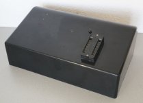
So, here is my suggestion for an EPROM adapter...

Wire a socket (for the EPROM) to a header plug pin for pin EXCEPT for the following:

EPROM pin 8 to header pin 10.
EPROM pin 9 to header pin 11.
EPROM pin 10 to header pin 8.
EPROM pin 11 to header pin 9.

This should keep the least significant 4 bits of the byte the same (so I can use them as check bits), and should swap over the top two bits of the data byte - so the character we get for each byte on the VDU display should now change.

I should then be able to reassemble each byte, with four bits acting as check digits (i.e. they should be the same as last time)...

Dave
 
Unfortunately, I think I have managed to disassemble as much as I can with 25% of the program missing! I just seem to have too many variables to make any further inroads. After a good nights sleep I may have some more ideas of course, but it would be much, much easier to have the remaining two bits of each byte to fill in the puzzle rather than guessing!

Dave
 
Back
Top