• Please review our updated Terms and Rules here

Need manual / jumper settings for Jameco JE-1043 FDC. Have newer ROM image.

In the process of unpacking, I discovered an earlier Version of the Jameco JE-1043 FDC
card that has a hardwired modification. The Hardware modification adds a LS7404N
stacked on top of the IC at U23. ONLY Pins 14 and 7 are soldered to the IC U23, and
all other Pins are bent away from the Pins of U23.

There is a wire from Z80 FDC Z0765 U25 Pin 26 to the added LS7404N Pin 13.
FDC9216B has Pin 5 Bent out so it does not go into the IC Socket. There is a wire
from LS7404N Pin 12 to FDC 9216B U24 Pin 5.

I haven't located any files with this Modification Information. Photo's are attached.
My PCloud has been updated, with this information.

Does anyone have the Jameco Documentation for this MFM/FM Update?

Larry
 

Attachments

  • IMG_20220726_102733490.jpg
    IMG_20220726_102733490.jpg
    683.6 KB · Views: 10
  • IMG_20220726_102805651.jpg
    IMG_20220726_102805651.jpg
    806.6 KB · Views: 10
  • FDC9216_ETC.pdf
    191.3 KB · Views: 2
  • Z0765A_Zilog.pdf
    1.1 MB · Views: 1
I may be the guilty party suggesting the mod quite some time ago. I've certainly done it on a number of old FDCs that used the 9216 data separator. However, I recall suggesting finding a spare gate on the board rather than piggybacking. I think I still have an old JDR controller (not an HD one) board with this modification.

As a matter of fact, that modification from around 1987 is still in the 22Disk documentation. It starts out thus:

Code:
      Modifying A PC-XT "Clone" Controller For Single-Density Reading

      Got a bunch of Xerox 820 diskettes that you'd love to be able to read?
      Sold your Osborne I at a swap meet and need your correspondence  files
      from 1981?  Too bad, your PC can't handle single-density diskettes...

      Or can it?

      Well, it can be done with a little patience, a few bits of wire, and a
      small  soldering  iron.    The result is a controller that remains PC-
      compatible as far as any DOS software can tell,  but has an  extra  FM
      mode in addition.

      Do  not  attempt  this modification unless you really know what you're
      doing and have worked with this kind of equipment before.   This is no
      place for a novice.

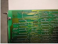
      First, you need to determine the type of controller you're using.  The
      original  IBM PC and PC/XT controllers are NOT readily adaptable,  but
      most inexpensive clones are.

      The important thing to locate on  the  controller  card  is  the  data
      separator chip; it's an 8-pin DIP.  It looks something like this:


                                     Page 23


                             +--U--+
                     Pin 1   |     | Pin 8
                     Pin 2   |     | Pin 7
                     Pin 3   |     | Pin 6
                     Pin 4   |     | Pin 5
                             +-----+

                           (Top View)

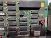
      This DIP (Dual Inline Package) will have pins 4,  5 and 6 grounded and
      pin 8 connected to the +5 supply trace.    Numbering  of  this  device
      varies  --  Western Digital (the prime source) has it as a WD 9216;  a
      NEC part number is UM 8326.   But it's all the same as  far  as  we're
      concerned.

      Identify  the  diskette  controller  chip on your board -- this is the
      large 40 pin DIP  labeled  uPD765A  (NEC),  Z765A  (Zilog),  or  8272A
      (Intel).   Note that pin 26 is a no-connection on your card -- this is
      the MFM/FM mode output pin.

      The last thing you need to find is an unused inverter section.    This
      is the most difficult part of this whole modification.  Most cards use
      a  SN7404 or 'S04 as an oscillator (look near the crystal).   Usually,
      not all sections are used.   Or look for a section of an 'LS00 gate or
      some  such  thing that can be wired as an inverter (Hint: tie both in-
      puts together).

      You need to lift pin 5  of  the  8-pin  data  separator  (above)  from
      ground.  Depending on how your card is laid out, this can be quick and
      simple (cut the ground trace) or very messy (unsolder the whole chip).
      Connect  a  wire  (wire-wrap wire is great) between this pin 5 and the
      output of the inverter which you located.   Connect a second wire  be-
      tween  pin 26 of the floppy disk controller (uPD 765) and the input of
      the inverter.

      That's it -- put the card back into your PC and  make  sure  it  still
      handles regular DOS diskettes okay.

      If  you've got an AT-style controller or a Western Digital 'Fox' dual-
      density XT controller,  you can even drive SD and DD 8" diskettes with
      this modification.

      Note  that  this  simple  modification will enable you to read single-
      density diskettes,  but not to write them.   If you're  really  adven-
      turous,  an  XT-style controller can be made to write diskettes if the
      write-precompensation circuitry is bypassed.   We do it  here  with  a
      section of a 74LS157 driven from the MFM pin of the '765.  A schematic
      of your controller is a must for this kind of work.

We're all haunted by our past deeds, it seems.
 
Last edited:
Chuck,
Now that all makes sense, and I likely used your Documentation in 22DISK to do the Modification.
I just didn't remember doing it, and would have never figured it out where I got the information.

THANKS AGAIN!.

Larry
 
A while back someone on the forum was selling some excess boards and I picked up one of these LCS-6610F controllers seemingly new in box, or at least in box. It's completely different from the ones shown here, and I've never used it so I don't know if it has the same functionality that the bigger cards do, but I figured I'd share what I've got in case someone needs the manual or ROM at some point in the future.

lcs-6610f_board.jpglcs-6610f_board_box_manual.jpg
 

Attachments

  • 27c64a.zip
    3.3 KB · Views: 6
  • Longshine LCS-6610F.pdf
    928.5 KB · Views: 7
So according to that data sheet it will do FM.

Edit: Or at least the chip will I guess.
 
On Post #11 it says:

JP2 JP3
CLOSED OPEN 3F0h to 3F7h
OPEN CLOSED 370h to 377h
NEVER JUMPER BOTH JP2 & JP3 AT THE SAME TIME!

What happens if you do??


Data seperator goes bad?
FDC controller IC goes bad?
Blowing up the PAL / GAL chips?

Are those PAL / GAL chips only for the high density part of the FDC?

And i like to know if someone can reverse engineer those PAL / GAL chips.. Or can make a tutorial how to do it your self.
 
Last edited:
Almost a dead certainty of reverse engineering--they appear to be combinatorial in nature; years ago I posted a step-by-step of how I re-engineered some selected PAL chips, so that's been done also.
And no--I'm not going to go through that again. Others have done the same.
My guess is that putting both jumpers on for the secondary and primary addresses will cause the FDC to respond to both, one or neither of the addresses. It will almost certainly not affect components on the card.
 
Is it a hard job doing both pals together, or is it just impossible? Or when trying they wont survive?
 
Iam guessing that those PAL wont have a long live, or can be dead in some sort time.
Is there anything possible to do, to get some replacement for it, if they will go bad.
 
Because all ICs will die because of age?

If a rom can be corrupted a PAL also can?
 
Back
Top