MattisLind
Veteran Member
BTW. When testing a germanium transistor one has to understnad that the readings will be quite different because of the lower forward drop. The forward drop is around 0.2-0.3 V rather than 0.6-0.7V.
You can easily test if it is germanium or not. Remove them and mesure the PN-junctions. If there are around 0.7V voltage drop on BE/BC it is silicon. If around 0.3V it is germanium.I have had a separate suggestion that the transistor marked B411 can't possibly be a germanium transistor, so that now makes two people telling me this. It is very clearly marked as B411, but if it isn't a germanium transistor what could it possibly be?
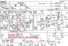
I have already replaced C439 and all the other electrolytics. I haven't been able to find a BU508D in a TO3 case so far, but it still remains to be seen whether my board really uses a BU407D as shown in the schematic, so not really sure it would be right to replace it with a BU508D anyway.In that schematic its a BU407D (with diode) , so any can do the job who suited in this TV type of fly-back circuit.
Used in many TVs back in the late 1970's, early 1980's.
So use the more common BU508D (8A amps) , they can be found in TO3 housing , or TO-247.
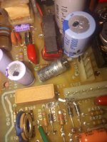
And! Beware of those old "Sparque" capacitors, they suspect of very leaky. Like C439
This is what I have found with the part removed using my diode tester. I also tested CR406 which has the same markings:You can easily test if it is germanium or not. Remove them and mesure the PN-junctions. If there are around 0.7V voltage drop on BE/BC it is silicon. If around 0.3V it is germanium.
But the marking on the chip shows that it is a Sanyo 2SB411. Not many alternatives.
| Joint | Q414 | CR406 |
| B-C | 2.7V | Open |
| C-B | 0.1V (beep for short circuit) | 0.1V (no beep) |
| B-E | 1.4V | 1.8V |
| E-B | 0.15V | 0.15V |
| E-C | 0.16V | 0.16V |
| C-E | 1.45V | 1.8V |
Yes, my next task is to draw the schematic. I have already done the Q414 side of T403, I now need to do the Q413 side which is where the main differences between my board and the schematic in the print setBTW. I think you should trace out the difference between your circuit and the schematic. Then it might be possible to understand why they use two germanium PNP-transistors to replace one silicon NPN-transistor.
This is what I have found with the part removed using my diode tester. I also tested CR406 which has the same markings:
Joint Q414 CR406 B-C 2.7V Open C-B 0.1V (beep for short circuit) 0.1V (no beep) B-E 1.4V 1.8V E-B 0.15V 0.15V E-C 0.16V 0.16V C-E 1.45V 1.8V
So it would seem to indeed be a germanium transistor, but the differences make me think that at least one of them is faulty. The apparent short circuit is the bit that is a bit concerning, not sure if the DMM is being fooled by the fact that it is not a silicon part and that it is testing fine as a germanium transistor.
You raise a good point. When I resurrected this thread I thought it would be OK given that it was about the same board. However, I have since wondered if I should have started a new thread too. Any thoughts and guidance for next time would be useful.Hello All and Happy Holidays to those who are celebrating...
As I am recovering from a bout with COVID and am not supposed to be out and about, I decided to tackle my own VT101 restoration project. Would it be appropriate to ask some questions of my own in this thread, or would that be considered hijacking? I want to be respectful to the original poster who started this thread...
Thanks, Jon.
As I think about it, it made sense for you to restart this thread, because the previous conversation had concluded successfully... otherwise there would be confusion about issues and answers. Since you are still in the middle of debugging your VT100, I think I will start a separate thread. Anyway, good luck with it!You raise a good point. When I resurrected this thread I thought it would be OK given that it was about the same board. However, I have since wondered if I should have started a new thread too. Any thoughts and guidance for next time would be useful.