• Please review our updated Terms and Rules here

PCB Reverse Engineering

pbirkel@gmail.com

Veteran Member
Joined
Apr 7, 2013
Messages
1,190
Location
Silver Spring, MD, USA
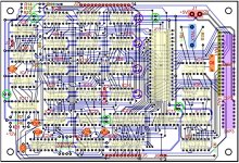
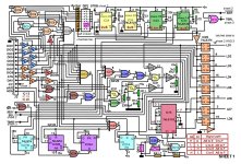
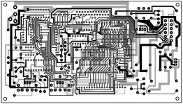
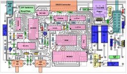
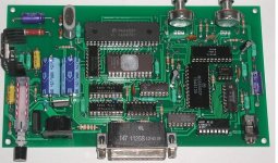
I find myself faced with the task of reverse engineering an undocumented 15x15" two-layer fully populated PCB. The bus into which it plugs is also undocumented. It's principally populated by MSI TTL, with some resistor packs, and lots of thin traces and vias. All of the ICs/packs are well-labeled common parts, so that's a plus. I do have general expectations regarding circuit functionality, but nothing particularly specific beyond power rails, bypass caps, and inferences associated with prominant ICs (CPU, SRAM, UART, RS-232 receivers/transmitters).

I've done some preliminary tracing, enough to realize that some important functional subcircuits are implemented using scattered ICs and long traces; my immediate problem being abnormal power-up reset behavior where the associated circuitry is quite elaborate and unintuitive (thus far). AFAICS I'll need to reverse engineer major areas of the PCB in order to suss out the reasons for the current behavior. I have several PCBs of comparable complexity that I'll eventually want to fully reverse engineer, so I'm contemplating the best way to go about the task. Not sure how to most effectively and efficiently apply "elbow grease".

All that I've read seems to reduce to using an ohm meter to confirm visual trace-and-via following with special fun where traces disappear under ICs. Then diagramming IC logic with identified connectivity. Then assorting logic into comprehensible patterns/subcircuits. Possibly having to go back and check for trace branching hidden under ICs where it seems that there may be missing logical connections. Then probing those logical subcircuits to ascertain signal patterns under operational conditions. Lather, rinse, repeat.

I'm interested in the approaches that others have used in this sort of scenario; means and methods, tools and techniques, time/effort savers, effective short-cuts, etc.

Thank you for sharing your advice and experience!
 
I understand that the latest / current version of the PCB design software KICAD has a mode where you can import a photo or scan of an original (unpopulated) PCB and then place another drawing 'layer' on top onto which you can effectively 'trace' the tracks of the original PCB, one-for-one, in order to make an exact copy of the original.

The analogy would be getting an original PCB, putting a piece of semi transparent 'tracing paper' over the top of it and then drawing over all of the tracks, pads and VIAs until you have a complete traced copy of the artwork of the original PCB, except this way you end up with an electronically 'traced' copy.

Of course this really only works well if you have an unpopulated PCB to trace from, so the question is, do you have an original PCB which you can sacrifice or carefully, temporarily uninstall every part from in order to do this? My guess would be probably not, as it will be a shortage of original PCBs which has triggered this need.
 
Of course this really only works well if you have an unpopulated PCB to trace from, so the question is, do you have an original PCB which you can sacrifice or carefully, temporarily uninstall every part from in order to do this? My guess would be probably not, as it will be a shortage of original PCBs which has triggered this need.
PCB originally produced in the early 1980's and I'm definitely unwilling to depopulate it. Plus I don't see how the vias would be handled without registration of the two sides, etc. Given the large PCB size there would a serious phase of trying to stitch together at least 4 sections. The component-side wouldn't work on a flat-bed scanner either, so probably more than 4 sections there. Then trying to get the two sides to register with each other. Maybe I can get a half-loaf from solder-side scans. I'll take a look at KICAD and see what it can do to help me out.
 
I don't see how the vias would be handled without registration of the two sides, etc.

I don't know the software but that would be such a fundamental requirement - to have not only the VIAs but all other through hole plated pads exactly matched up on both sides - that I am sure the software will have a way of handling it.

I think if I was trying to do this I would start by either scanning or photographing the solder side for a reference to where all of the VIAs and other through-holes are, since these are by definition in exactly the same place on both sides of the PCB - if you place them in the right place on the solder side then they will be in the right place, suitably mirrored, on the component side as well.

To illustrate this, consider a small double sided PCB with just one DIP IC and associated components on the component side. On the solder side all of the tracks and their routes are visible.

If you start by placing a set of IC pads on the solder side layer and as you do so, specify that they are through-hole, the software should automatically create a second component-side layer on which the top sides of those IC pads have been created in the correspondingly correct place. Continue adding through-hole pads, vias and so on on the solder side layer and the software will continue to populate the top side layer with the component-side ends of those same pads and vias.

Eventually you end up with a solder side layer where you have placed all of the pads, vias and so on and joined them up with solder side tracks so your solder-side is an exact copy of the solder side of the original PCB. Meanwhile the component side layer will now have an array of IC pads, component pads and VIAs on it, not joined together by anything. This would be the point where, if you are not willing to depopulate the PCB, you have to do a lot of painstaking manual and visual tracing so that you can draw in all of the missing component side tracks manually.

One other thing I would ask - it sounds as though these PCBs could be large enough to have microprocessor or microcontroller circuitry on board - if they have conventional microprocessors with separate EPROM, RAM, etc then retrieving the program code for use in any subsequent clone should not be a problem but if the code which runs the PCB is in a microcontroller, especially a mask programmed microcontroller, it may not ever be possible to make a clone work - except by pulling a hopefully good original microcontroller from a dud original PCB.
 
I have reverse engineered a number of vintage pcb designs, including those for computers. This is my advice:

One was the Cromemco Dazzler:

www.worldphaco.com/uploads/THE_WORLD_FAMOUS_CROMEMCO_DAZZLER.pdf

And the Votrax Type 'N Talk:

www.worldphaco.com/uploads/VOTRAX_TYPE___TALK_MEETS_HERO_JR.pdf

and a replica personality module for the SOL-20:

www.worldphaco.com/uploads/Personalityreplica..pdf

Then, finally I progressed to an exact replica of a 4 layer pcb, though in this case I had to create the two internal layers:

www.worldphaco.com/uploads/THE%20RM65%20CRTC%20MODULE%20AND%20THE%20AIM.pdf


You can look at these articles and see if you think I did a good job replicating them, or not.

When the Apple 1 pcb was re-created by some, the designers fouled it up because they did not create the exact track pattern of the original pcb. While it worked, after a while they realized, if you really want to do better with a vintage replica, you had better make it an exact match. This requires a lot more more work & effort. Not using a track auto router.

The key thing is to make them "exact replicas" if you want them to work properly as the originals did and look identical.

Forget about trying to simplify the logic with FPGA's too. You will dig your own grave with unexpected timing anomalies.

Stick to the original 74 series chips of the same sub-type. Don't think about changing the track design either and completely forget about a track auto-router that works from a schematic capture, that you think might save you time.

Don't switch to IC types such as HC & HCT, F etc or anything else than the original parts, or all that you will do is open a can of timing worms and induce a range of faults that are very hard to resolve. Also, with other passive components, try to keep them as close to the original parts as possible. In some cases you might have to hunt down the original parts, crystals, ceramic tuning capacitors etc.

To get it right requires the foil patterns of the original pcb's are also are an exact match. Photos work for this, and then you also require the original schematics for checking.

My approach was to draw over the top of the original foils/photographs, in a transparency mode in a photo editor (I use vintage Microsoft Picture IT) with a background 2.54mm grid. Most of these old pcb's were designed on this grid pattern. I then create the two sides of the board as a jpg image, though more lately I have been doing it in Kicad, because it saves the pcb maker having to convert my jpg's to Gerbers.

I know I have succeeded when the pcb I create is an exact match for the original, but don't hold back on the Gold plating, even if the originals did not have it.

Also, to get the more complex boards correct, like the two Cromemco Dazzler boards and the RM-65 video card, I can promise you that I had to stay up many late nights burning the midnight oil, to make 100% sure they were correct and there were no errors at all. So be prepared for that, depending on the complexity of your project.

If your board is undocumented, you will need to copy out the schematic, manually as I did in this undocumented case:


This case involved copying out the pcb pattern from the actual board and re-generating the undocumented schematic with the aid of the IC data sheets.

But I am no stranger to this problem For example I acquired some Avionics VDU's with no available manual, so I simply copied out the entire schematics by hand. In this case I also discovered a very interesting black level clamp circuit, that turned out to have been invented by Tektronix. Sometimes the lesser travelled road and more difficult one leads to more interesting findings:

www.worldphaco.com/uploads/The_1987_Vintage_Avionics_Conrac_Video_monitor..pdf
 
Last edited:
If you start by placing a set of IC pads on the solder side layer and as you do so, specify that they are through-hole, the software should automatically create a second component-side layer on which the top sides of those IC pads have been created in the correspondingly correct place. Continue adding through-hole pads, vias and so on on the solder side layer and the software will continue to populate the top side layer with the component-side ends of those same pads and vias.
I was thinking about the possibility of creating labeled vias (as well as through-hole IC pads) as a starting point for moving from a solder-side scan to working the component-side manually. Fortunately this is oldish-tech and everything is through-hole.
Eventually you end up with a solder side layer where you have placed all of the pads, vias and so on and joined them up with solder side tracks so your solder-side is an exact copy of the solder side of the original PCB. Meanwhile the component side layer will now have an array of IC pads, component pads and VIAs on it, not joined together by anything. This would be the point where, if you are not willing to depopulate the PCB, you have to do a lot of painstaking manual and visual tracing so that you can draw in all of the missing component side tracks manually.
Your observations are good confirmation that such an approach might accomplish a half-loaf, followed by at least some better-organized manual tracing :-}. Thus far I've only tried to manually trace the reset circuitry and doing so has given me a healthy respect for the necessity of a campaign plan!
One other thing I would ask - it sounds as though these PCBs could be large enough to have microprocessor or microcontroller circuitry on board - if they have conventional microprocessors with separate EPROM, RAM, etc then retrieving the program code for use in any subsequent clone should not be a problem but if the code which runs the PCB is in a microcontroller, especially a mask programmed microcontroller, it may not ever be possible to make a clone work - except by pulling a hopefully good original microcontroller from a dud original PCB.
The only "burned in data" is a socketed bipolar ROM that will be easy to read, and that's on a second PCB that I'll also need to tackle. To some degree I'm operating in a sweet spot where the use of VLSI is limited to pretty well documented industry-standard parts, and the remaining circuitry is either jelly-bean MSI or discretes -- all industry standard. No opaque house numbers :-}! It's principally the extent of the MSI that is daunting; it doesn't appear to follow the usual conventions/expectations for a bus-oriented system ... although it does have plenty of external bus-like signal lines. That it's a 16-bit CPU tends to double the number of ICs and traces to track; only the SRAM follows a nice ordered pattern.
 
I have reverse engineered a number of vintage pcb designs, including those for computers. This is my advice: ...
Thanks Hugo. I've enjoyed and appreciated your many recoveries and recreations. Fortunately I have no interest in replicating these boards -- I just need to regenerate their schematics as a step towards understanding their operation ... and then hobbyist reuse.
 
I'm interested in the approaches that others have used in this sort of scenario; means and methods, tools and techniques, time/effort savers, effective short-cuts, etc.
My biggest task was re-engineering a Datapoint 5500. My approach: I created a schematic and placed the ICs as good as possible in the same spot in the schematic as on the board but with a lot of room between them. And then I drew the connections between ICs using the lanes between the ICs.
I had one big advantage: the guy who owned the board had a second one and was able to make a X-ray of it. That meant a lot less stress to find out where lines between the board and IC went to.

Good luck!
I was fortunate too, in that the RM-65 video card, I was able to see the X-ray. This helped create the two middle layers, one had a data bus in it, it was not just the ground and + power distribution, which it often is.
 
Thanks Hugo. I've enjoyed and appreciated your many recoveries and recreations. Fortunately I have no interest in replicating these boards -- I just need to regenerate their schematics as a step towards understanding their operation ... and then hobbyist reuse.
Ok, I thought you actually wanted to make replica boards.

In the case you just want to acquire the undocumented schematic, doing it again I would use the method that I used for the Taylor-Wilson unit.

Once I had copied the track design, I created a dual layer transparency to see both layers together, then another transparency with the IC's on it, but with the internal IC structure from the IC data sheet for most of the IC's, showing the gates or IC internals. I made each IC image from the data sheet of it, and scaled it to fit. For some of the IC's this was not practical and I used their data sheet.

Then I could see everything at the same time on one sheet. (image attached, look closely and you will see the internals of most of the IC's)

But I found, that an A4 sheet size for this application was too small. So I took it to a print shop and they printed onto a large sheet. Then I was able to sit down and copy the entire schematic out from that, then draw it neatly in the drawing program.

You will find that it might take one or two iterations of schematic drawing at least, before you end up with the final one. The reason is, schematics are often drawn by the designer who understands the circuit sub-sections and the flow of signals via the circuit. You have to reach the target first of figuring out how the circuit works, then it aids drawing a sensible looking circuit that represents the signal flow, in a general left to right fashion, without things like gates pointing in multiple directions and connections cris-crossing back and forth across the diagram and a real mess. Also, the schematic for the TW unit would not fit on one sheet of A4 and it needed 3 sheets for neat drawings so that everything could be seen clearly and also broken up into functional parts, otherwise the different sheets would end up with too many interconnections and gates etc that really belonged on another sheet. Attached an example of just one of the three sheets. Obviously this was not my first attempt after copying it out.
 

Attachments

  • TWPCB.jpg
    TWPCB.jpg
    621.6 KB · Views: 15
  • TWPCB2.jpg
    TWPCB2.jpg
    386.8 KB · Views: 14
Last edited:
Once I had copied the track design, I created a dual layer transparency to see both layers together, then another transparency with the IC's on it, but with the internal IC structure from the IC data sheet for most of the IC's, showing the gates or IC internals. I made each IC image from the data sheet of it, and scaled it to fit. For some of the IC's this was not practical and I used their data sheet.

Then I could see everything at the same time on one sheet. (image attached, look closely and you will see the internals of most of the IC's)

But I found, that an A4 sheet size for this application was too small. So I took it to a print shop and they printed onto a large sheet. Then I was able to sit down and copy the entire schematic out from that, then draw it neatly in the drawing program.
That first image is really, really nice, especially with the portrayal of device-internal logic which graphically bridges from the simple trace layout to the circuit schematic. My manual experiment ended up somewhat along that line-of-attack as I tried to follow traces understood as circuit connections among specific logic devices with constant references to device-documentation. Pencil-and-paper quickly became a mess, and going back and forth between pin numbers and logic devices was clearly going to be a recurring point for the introduction of error.
You will find that it might take one or two iterations of schematic drawing at least, before you end up with the final one. The reason is, schematics are often drawn by the designer who understands the circuit sub-sections and the flow of signals via the circuit. You have to reach the target first of figuring out how the circuit works, then it aids drawing a sensible looking circuit that represents the signal flow, in a general left to right fashion, without things like gates pointing in multiple directions and connections cris-crossing back and forth across the diagram and a real mess.
Rational organization and decomposition of subsystems is going to be a necessity to get an intelligent layout for more than small circuits, and even then it's not difficult to lay out a small circuit incomprehensibly. I'm reminded of my many years of creating UML diagrams of complex data models and the problem(s) of laying them out in a comprehensible manner ... and the problem of limiting/avoiding line-crossing. There be dragons here ...

Also, the schematic for the TW unit would not fit on one sheet of A4 and it needed 3 sheets for neat drawings so that everything could be seen clearly and also broken up into functional parts, otherwise the different sheets would end up with too many interconnections and gates etc that really belonged on another sheet. Attached an example of just one of the three sheets. Obviously this was not my first attempt after copying it out.
I imagine that you first went through a phase of "dispersal and organization" in order to understand the overall functioning of the circuitry and implied subcircuits, and then a phase of "layout compaction" to achieve a set of coherent schematic sheets with limited sheet-crossing signals?

Roughly how much effort did you end up investing in this particular project and what steps consumed most of it?

I spent yesterday starting to learn KiCAD 7, a task that I've put off much too long. What it now seems to be able to do is derive a netlist from a PCB layout, and then use the netlist to create a (messy) schematic, rather than the usual schematic->netlist->PCB layout flow. An example of this process is demonstrated in (poor audio!):


I'm going to try this with a smaller 5x11" PCB from the same system (29 ICs, 26 switches, 35 LEDs, dozen discretes, plus bypass caps and a 2x25 connector) to see how well it works out and how long it takes an inexperienced fellow like myself. It looks very promising, particularly as a means to cut down on manual errors.

Hidden traces under components remains an unavoidable problem. Particularly long-run traces under multiple ICs that may shift position as they pass under devices, perhaps branching there as well. And possibly a hidden via involved. Oh for a clean PCB to work from!
 
Last edited:
When I did the Taylor Wilson, no thought of pcb software or Kicad was involved. It was all old school drawing and circuit theory.

If I wanted to actually manufacture pcb's though, I would draw what I documented into Kicad. The simple reason being, it is cheaper. In the past I had simply sent my .jpg images of the pcb to the software house and they transcribed it, but of course that attracted an engineering fee from the pcb company.

With regard to hidden traces, I found this out with the Type 'N Talk replica (see attached images). The photos I had of the original pcb, concealed the tracks under the IC's & sockets.

But, I found I could resolve all of them, from the position of the tracks entering the periphery of the IC socket.

But for a case like that, to avoid fouling it up, the schematic is required. Unless of course you have the original pcb sitting in front of you on the bench. In that case you can sound the connections out with a meter.

Notice on the pcb, the early style axial electrolytics, the interesting pale green axial ceramic 0.1uF capacitors (made by the Corning Glass Works) and the identical power switch and type of long reach serial connector that the original unit used.

All of these very small (and seemingly insignificant details) things are very important, that is if you want an exact replica. It takes a while to hunt these down to make the replica.

One of my more interesting replicas is the 20.005 MHz Transmitter used in the Russian Sputnik-1 Satellite. It was a tough job to track down all of the interesting Russian parts, including the tubes, the manipulator relays and the Russian resistors, capacitors etc. Apart from that one of the most difficult parts was replicating the mechanical hardware. Often you will see a lot of projects where the circuit design is good, but the mechanical considerations are out the window.

Anybody interested in early space exploration might be interested in my article. It was quite a job to create an exact replica, also I had to make a power supply to power it. The only other "replicas" I have seen were "hopeless" on veroboard, and nobody at all bothered to investigate one of the most astonishing parts of it, the Manipulator, which, composed of magnetically latching relays, consumed less than 20mW of power, it is quite astonishing. To replicate the hardware I used CNC cut brass panels. I had to learn how to cut ceramic tube and also to make a replica glass enclosed Crystal:

www.worldphaco.com/uploads/THE%20SPUTNIKSTORY.pdf
 

Attachments

  • TNT1.jpg
    TNT1.jpg
    308.8 KB · Views: 9
  • TNT2.jpg
    TNT2.jpg
    311.6 KB · Views: 9
  • TNT3.jpg
    TNT3.jpg
    355.2 KB · Views: 10
Last edited:
Hugo's work really is outstanding, well done.

I'm only a bystander interested in this thread but a little while ago Jerry Walker showed how he traced a front and back PCB photo to reproduce a card for a Hazeltine terminal, which had curved traces:
https://www.youtube.com/watch?v=YeEP9vVMfx4
I reckon the software he used would be great to repop some Unibus flip chip boards.

I was wondering if an HP 547A current tracer probe coupled with a signal injector could possibly be used to find the locations and paths of traces that go under chips, or is X-raying the only reliable way to find out?

It is fairly easy to figure out where the tracks hidden under IC's go. This was required to the Votrax type & Talk replica, because all I had were the pcb photos from the internet and the schematic that somebody else had copied, there was only one error in their schematic, it turned out. You have to be careful if you are working with somebody else's schematic and not the manufacturer, though they are not guaranteed to be error free, this is why it is important to figure out how the circuit works, that can expose errors. When the tracks go under the IC from the ends and between pins, there are only so many places they can go and they don't cross over each other, if they do you can see the vias and tracks on the bottom of the board (unless a 4 layer type). I simply used the meter to & schematic to resolve it.

One thing that could upset the apple cart would be if there are surface mount parts under the IC. You can run cardboard spacer under the IC to check. If they were there, and especially if there was an over-lying ceramic body IC, that would be a challenge because the ceramic is very radio opaque on X-rays. Fortunately, most vintage computer pcb's at least from the 1970's era don't tend have surface mount parts, though they existed at the time mil spec gear.

When I replicated the Dazzler pcb's I thought at one point that I had discovered an error in Cromemco's documentation, because they had an output, connected to the output of another IC on the board . However, when I looked up the IC, it was a type of flip flop design where one of its outputs was connected to an input of a gate on the IC die. So you could get this particular flip flop to change state by forcing its output, and this does not damage it, because it is only forced for the small time it takes to change state. I had not seen this commonly done before, though there is another example of it: A common switch de-bounce circuit using a pair of inverter gate uses the same approach.
 
Last edited:
You have to be careful if you are working with somebody else's schematic and not the manufacturer, though they are not guaranteed to be error free, ...
Definitely. Examples:
1. Some errors in IBM's circuit diagrams for the PC series are listed at [here].
2. SAMS Computerfacts CSCS17 (for early IBM AT) has the values of crystals Y1 and Y2 swapped.
 
Definitely. Examples:
1. Some errors in IBM's circuit diagrams for the PC series are listed at [here].
2. SAMS Computerfacts CSCS17 (for early IBM AT) has the values of crystals Y1 and Y2 swapped.
Then there are manufacturing hardware errors too.

In the case of the Votrax type and talk they left out a section of track on the pcb, and as fate would have it, the defect it caused din't stop the unit from working, so nobody noticed !

In the original Atari Arcade Pong PCB, with about 65 IC's, the pcb designer made a mistake because the pin numbering was incorrect on one of the IC's on the schematic Atari provided him with. This swapped the least significant bit of the player paddle data, so the position of one player's paddle influenced the interaction with the ball on the other players' paddle. The created a spooky effect and later got called "The Ghost in the Machine". The problem was accidentally rectified when they made the Pong Doubles version of the game and the original mistake did not come to light for over 40 years and even surprised the designer.

I have an interesting Eddystone shortwave radio from the 1940's era. When I was aligning it I found one of the RF transformers did not peak normally. They had arranged these in rows, with wire links soldered from their pins, to the band change switch. One link was never fitted at the factory (must have been Friday) but it got through their alignment and quality control systems. Somebody was not paying attention.

Other things I have found are; electrolytic caps fitted in reverse from new. In one case a diode in a CPU circuit and under certain conditions only, the device would malfunction.
 
It is fairly easy to figure out where the tracks hidden under IC's go. ...
Well, it's tedious, and there's a non-nice complexity growth problem when multiple ICs are involved as the multiplicity of where-might-it-go grows significantly with each passage. On a 15x15" board with a solder mask and long traces I assure everyone that it becomes quite challenging after a half-dozen ICs and a couple of vias as until reaching a connected pin or via you're at the mercy of the combinatorics. But, yes, it can be done ... especially with MSI where there's a fairly limited routing space and no possibility of hidden parts. 0.600" parts with large pin counts raise the multiplicities significantly.

Unfortunately KiCAD 7 can't actually generate a netlist from a PCB. AFAICS there's no technical restriction to doing so given recent functional improvements, just a matter of programming effort for which there's apparently been no implementation volunteer as the use-case is sufficiently infrequent. As matters currently stand it's a domain-aware, electronic light table -- full of helpful features but not an end-to-end solution. Maybe someone will take up the challenge of adding the missing bit in a future release.
 
Jerry Walker showed how he traced a front and back PCB photo to reproduce a card for a Hazeltine terminal, which had curved traces:
https://www.youtube.com/watch?v=YeEP9vVMfx4
Thanks for pointing this out. The reverse engineering segment starts at about 5:30. The tool used, Easy-PC, is professional-grade (https://numberone.com/downloads/datasheets/Easy-PC Brochure.pdf) and fairly expensive for the hobbyist ($300-$500 USD). Alas the trial version is unable to save files, rather than simply being pin-count limited, although I suppose that one could take happy-snaps of the resulting schematic for later reference.
 
Well, it's tedious, and there's a non-nice complexity growth problem when multiple ICs are involved as the multiplicity of where-might-it-go grows significantly with each passage.
Yes that is the thing. To do it you have to be a relentless die hard, stay up late, burning the midnight oil (when everybody else is either sleeping or at a party). I learnt the lesson many years ago, in some cases there is no escaping elbow grease and a lot of hard work, if you want an excellent result that is. For this sort of work, quick computer generated solutions are more of a pipe dream.
 
I didn't understand why the component side would be more difficult to scan in a flatbed scanner than the solder side unless there were components taller than resistors and ICs, in which case if there were few of them I'd remove them temporarily to do the scan. I have usually had reasonable success using scans of both sides of a board overlaid in transparency mode in a graphics package and the layers can be distorted to make the vias align. Also I use the graphics tools to draw lines along the traced paths in a separate layer so that I know which tracks I have already recorded.

However, my simpler approach is just to shine a powerful torch through the PCB so that the outlines of the tracks on the underside are visible on the component side. It's really a matter of using every technique in combination and including a fair amount of intuitive guesswork.

Now if anyone can suggest how to trace wires that disappear into a thick cable harness containing many wires all the same colour when those traced wires don't appear to come out anywhere that I can get a test probe to, that would be a great help. Oh for a simple flat PCB to analyse!
 
Back
Top