• Please review our updated Terms and Rules here

PET 8032 - No Chirp, No Cursor

Look on the schematics for the /CAS0 and /CAS1 signals. /CAS0 drives the lower bank of RAM (odd-numbered UA devices) whilst /CAS1 drives the upper bank of RAM (even-numbered UA devices).

It may not be the RAM itself of course - the data bus buffers are notorious for failing, as are the address multiplexers. I have also seen the refresh counters fail - this causes some 'interesting' faults!

Dave
 
See what happens when I go to bed!

Have you run my PETTESTER DRAM test program - this runs after the counter counts down to zero.

Dave
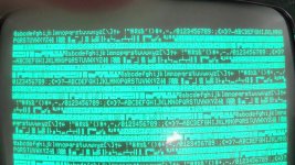
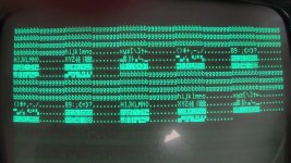
No, it still won't run with the 8032's onboard RAM. I get the following two patterns, and no change afterwards. Is there anything here that reveals any information? I had planned to just start unsoldering RAM.

PETTETST_1.jpg

PETTETST_2.jpg
 
Please don't just start wielding the soldering iron...

There is a pattern there - let me analyse it for you first...

It looks like 8 bad memory cells followed by 8 good memory cells. The data for the bad cells looks almost correct - but has data bit 3 SET instead of CLEAR.

This looks to me like DRAM UA13 output being stuck HIGH.

If this IS stuck high - then piggybacking a DRAM on UA13 should work to prove it.

If it is not UA13, it could be the buffer at UB10.

Dave
 
Please don't just start wielding the soldering iron...
LOL, I'm a bit of a hack, but hopefully I haven't come off quite THAT ham-fisted! But I understand. I'm at work right now, so it will be 6-7 hours before I can look at it again. We're GMT-5 here, so you'll probably be in bed by then!
There is a pattern there - let me analyse it for you first...

It looks like 8 bad memory cells followed by 8 good memory cells. The data for the bad cells looks almost correct - but has data bit 3 SET instead of CLEAR.

This looks to me like DRAM UA13 output being stuck HIGH.

If this IS stuck high - then piggybacking a DRAM on UA13 should work to prove it.

If it is not UA13, it could be the buffer at UB10.

Dave
That's fantastic, thanks for that level of detail! If your documentation for the PETTEST explained all this, I beg your forgiveness for not understanding it completely. Also, I had tried the piggyback test early on, but there were so many other things wrong that it was probably not useful at that time.

I'll keep you posted.
 
Well, a lot of good things happened last night when I was in bed :)...

Let's hope we get a similar success tonight!

Dave
 
If a DRAM output pin is stuck high or low, generally piggybacking won't help, as the stuck output pin interferes with the piggybacked chip. In the case that a DRAM IC is "non responsive" though and its output pin is not being tri-stated with data, the chip behaving as though it is "not there" then piggybacking will work as a diagnostic technique. Both types of IC failure, "stuck output pins" or" non responsive" can happen with failed 4116's.

Generally for testing the DRAM IC in the PET my feeling is that it is better to actually test the DRAM IC's in the computer (with whatever system is devised), not only for the reason the chips are often soldered in. Even in sockets I have concluded it is better for this reason:

The PET designers knew about the complex timing foibles of DRAM, but the designers of DRAM testers are not always so clever it appears. For example I bought two new DRAM testers on ebay that test 4116 DRAMs with the seller's "homegrown" code in their micro's. One of the testers malfunctions when fast specimens of the IC's are tested and reports them as faulty, when they are not and are actually superior IC specimens. The other tester "appears ok" so far, but I trust the designers of the PET computer much more to put these complex DRAM IC's into their correct timing environment for testing. And, also, after all, it is important that the DRAM IC's work properly in the actual computer.
 
........also it is worth reading pages 11 & 12 of the article link I posted about this issue on post #38:

There is an interesting complication that one needs to be prepared for when interpreting the results of defective byte values returned from memory testing:

It could be tempting to think that if an IC was either non responsive, or had an open circuit output pin (its tri-state output not working or effectively tri-stated off) then the logic state would be assumed to be high, because it is feeding a 74LS244 TTL buffer IC and normally the inputs of TTL IC’s, when left open circuit, assume a high logic level. But, they don’t over a short time frame of a few uS (and due to the nature of the'244 IC's inputs). It takes time for an input pin to charge to close to a high logic level, when left “floating”. Testing indicates that the voltage level seen at the 4116 IC’s output pin 14, when it is tristated off, or open circuit, is a borderline logic level, depending on the timing.

So one needs to be “mentally prepared” for this variation when interpreting byte results returned from memory, while trying to figure out which IC is defective. If Commodore had used something like 10k pull up on the data outputs of the 4116 DRAM IC’s, this interesting ambiguity may have been avoided .

Also as noted there (excluding refresh failures), there are essentially 4 basic ways the DRAM can misbehave.
 
If a DRAM output pin is stuck high or low, generally piggybacking won't help, as the stuck output pin interferes with the piggybacked chip. In the case that a DRAM IC is "non responsive" though and its output pin is not being tri-stated with data, the chip behaving as though it is "not there" then piggybacking will work as a diagnostic technique. Both types of IC failure, "stuck output pins" or" non responsive" can happen with failed 4116's.

Generally for testing the DRAM IC in the PET my feeling is that it is better to actually test the DRAM IC's in the computer (with whatever system is devised), not only for the reason the chips are often soldered in. Even in sockets I have concluded it is better for this reason:

The PET designers knew about the complex timing foibles of DRAM, but the designers of DRAM testers are not always so clever it appears. For example I bought two new DRAM testers on ebay that test 4116 DRAMs with the seller's "homegrown" code in their micro's. One of the testers malfunctions when fast specimens of the IC's are tested and reports them as faulty, when they are not and are actually superior IC specimens. The other tester "appears ok" so far, but I trust the designers of the PET computer much more to put these complex DRAM IC's into their correct timing environment for testing. And, also, after all, it is important that the DRAM IC's work properly in the actual computer.

Agreed. I have had TWO DRAM testers, and I've found them to be unreliable. The Backbit tester is better and more versatile, but for DRAM, I still don't trust it as much as the actual computer it's working in.
 
Please don't just start wielding the soldering iron...

There is a pattern there - let me analyse it for you first...

It looks like 8 bad memory cells followed by 8 good memory cells. The data for the bad cells looks almost correct - but has data bit 3 SET instead of CLEAR.

This looks to me like DRAM UA13 output being stuck HIGH.

If this IS stuck high - then piggybacking a DRAM on UA13 should work to prove it.

If it is not UA13, it could be the buffer at UB10.

Dave
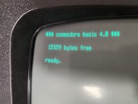
Ok, so I piggybacked UA13, and got different results. The screen was still garbled, but the behavior changed, and it looked like the test was running. So I replaced UA13, and now the system boots. So that's good news....sort of. But only half of the RAM is detected. When the PETTEST DRAM test starts, it identifies as only 16K. But this is continued progress!

NOTE: I neglected to check whether UA13 output (looks like pin 2 and 14 are tied together from the schematic) was stuck high, so after replacing it, I put the original back in, just for my own curiosity, and it wasn't stuck high. In fact, I checked the output of ALL the DRAM, and none were stuck either high or low. For what that's worth....


20220926_205637.jpg
 
Last edited:
Ok, so I piggybacked UA13, and got different results. The screen was still garbled, but the behavior changed, and it looked like the test was running. So I replaced UA13, and now the system boots. So that's good news....sort of. But only half of the RAM is detected. When the PETTEST DRAM test starts, it identifies as only 16K. But this is continued progress!

NOTE: I neglected to check whether UA13 output (looks like pin 2 and 14 are tied together from the schematic) was stuck high, so after replacing it, I put the original back in, just for my own curiosity, and it wasn't stuck high. In fact, I checked the output of ALL the DRAM, and none were stuck either high or low. For what that's worth....


View attachment 1246684

I explained in my article that this effect is what you get when one (or more) of the IC's in the upper 16k is non responsive.

What happens is at the boot up, BASIC goes to examine the RAM and writes and reads values from it. If there is not the same byte read as was written above the 16k threshold (address 3FFFh) BASIC assumes there is only 16k memory installed.

What this means is that the faulty DRAM IC/s are in the upper 16k bank. And they do not have a stuck output pin (or it wouldn't have booted), but instead the defective IC/s are "non responsive".

To find out which one it is, all you have to do is to write into memory above 3FFFh, (but in decimal using POKEs) and PEEK's (or the M/L monitor instead of PEEKs), of byte values 00 (0), FF(255) and another value like AA(170). You will soon be able to determine which IC/s in the upper bank are faulty from the returned byte value (It is all in the article with examples of how to do it)
 
Last edited:
This trick works - things move on when I go to bed :)!

What I should have said is that the output from the DRAM is always reading HIGH. The data will only be present on the DRAM data output pin when a READ occurs. As a result - in order to detect this problem - you need a trigger that will indicate what the data pin state is when the /CAS signal is LOW and the R/nW signal is HIGH. You will also observe the data being written into the RAM - as this is a common pin. This further confuses the human observer...

My PETTESTER is trying to find the top of memory by performing a quick test. What it has done is to detect a fault in the very first byte of the upper 16K bank of memory. It therefore assumes that only 16K is fitted to the machine.

I would suggest leaving my PETTESTER testing the lower 16K bank of memory for a while. Get 20 or so good passes and you should know you are good to go...

If you can get BASIC up and running - you can perform your own POKE and PEEK test on the upper 16K bank of memory to see where the fault is.

There is another (smarter) way that Hugo came up with. That is to exchange the /CAS0 and /CAS1 signals on the memory and let PETTESTER do its job again. The upper (faulty) 16K of memory then becomes the lower 16K. Don't forget to swap the signals back again though when you are done!

Positive progress is always good!

Dave
 
Goodmorning, i had similar problem with my old 8032 PET...I solved it by replacing a 6520!
 
That's on the basis that the cursor isn't flashing of course. Is that the case, or did the photograph get taken when the cursor was OFF?

Dave
Yes, the cursor is flashing. Sorry guys, I didn't notice that, or I would have mentioned it.
Hi Desperado....yeah....we're several days into this repair. I've actually replaced BOTH 8520s. Oh, and I need some, if anyone has them for sale. Do the non-MOS branded ones work? I saw them on Ebay somewhere.
 
I explained in my article that this effect is what you get when one (or more) of the IC's in the upper 16k is non responsive.

What happens is at the boot up, BASIC goes to examine the RAM and writes and reads values from it. If there is not the same byte read as was written above the 16k threshold (address 3FFFh) BASIC assumes there is only 16k memory installed.

What this means is that the faulty DRAM IC/s are in the upper 16k bank. And they do not have a stuck output pin (or it wouldn't have booted), but instead the defective IC/s are "non responsive".

To find out which one it is, all you have to do is to write into memory above 3FFFh, (but in decimal using POKEs) and PEEK's (or the M/L monitor instead of PEEKs), of byte values 00 (0), FF(255) and another value like AA(170). You will soon be able to determine which IC/s in the upper bank are faulty from the returned byte value (It is all in the article with examples of how to do it)
I DID look through your article briefly, but it's pretty dense, and maybe a bit over my head. But learning how to do the PEEKS and POKES into memory would probably be a good thing to know, so I will read it more thoroughly when I get time, and see if I can understand it all!
 
This trick works - things move on when I go to bed :)!

What I should have said is that the output from the DRAM is always reading HIGH. The data will only be present on the DRAM data output pin when a READ occurs. As a result - in order to detect this problem - you need a trigger that will indicate what the data pin state is when the /CAS signal is LOW and the R/nW signal is HIGH. You will also observe the data being written into the RAM - as this is a common pin. This further confuses the human observer...
Ah, yeah that makes sense. By 'stuck high' it doesn't mean what I was thinking.
My PETTESTER is trying to find the top of memory by performing a quick test. What it has done is to detect a fault in the very first byte of the upper 16K bank of memory. It therefore assumes that only 16K is fitted to the machine.

I would suggest leaving my PETTESTER testing the lower 16K bank of memory for a while. Get 20 or so good passes and you should know you are good to go...
I will do that tonight.
If you can get BASIC up and running - you can perform your own POKE and PEEK test on the upper 16K bank of memory to see where the fault is.

There is another (smarter) way that Hugo came up with. That is to exchange the /CAS0 and /CAS1 signals on the memory and let PETTESTER do its job again. The upper (faulty) 16K of memory then becomes the lower 16K. Don't forget to swap the signals back again though when you are done!
I told Hugo that I would give his document another careful read and see if I can figure it out. It's a little bit over my level but like I told him, learning to POKE and PEEK areas of memory is a good skill to learn, and I should probably do it. As far as switching /CAS0 and /CAS1, THAT I can definitely do, and I get exactly how that would work.
Positive progress is always good!

Dave
 
The BASIC statement and function of interest are:

POKE address, value
= PEEK( address )

If we want to play with address $4000 (the first byte of the second bank) this is (decimal) 16384.

So you can do:

10 A = 16384
20 POKE A, 0
30 PRINT PEEK( A )
40 POKE A, 255
50 PRINT PEEK( A )
60 END

This will set the first byte of the second bank to 0 and 255 and print the result of the POKE out in between. Any departure from 0 and 255 would indicate a problem.

You can get a bit more 'smart' by putting the above code into a loop, so you iterate around poking a value between 0 and 255 into a memory location and checking the result at each iteration:

10 A = 16384
20 FOR B=0 TO 255
30 POKE A, B
35 C = PEEK(A)
40 IF C <> B THEN GOTO 100
50 NEXT B
60 PRINT "ALL OK"
70 END

100 PRINT "ERROR"
110 PRINT "ADDRESS ", A
120 PRINT "SHOULD BE ", B
130 PRINT "FOUND ", C
140 END

Obviously you can test a range of memory addresses by putting A in a loop as well. But, beware, BASIC can be slooooow...

Dave
 
Obviously you can test a range of memory addresses by putting A in a loop as well. But, beware, BASIC can be slooooow...

Dave
This is why later I became accustomed to checking the memory contents using the M/L monitor , rather than BASIC PEEKS & POKEs, as it is super fast by comparison. To check the entire memory from 0400h to 7FFFh , watching the bytes of a checkerboard pattern scroll by, it takes about 4 minutes, but that is not excessive. For short blocks or memory pages it is very brisk.
 
Last edited:
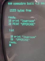
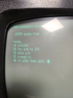
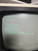
Well, shoot. Dave, I tried to type in your program, and found something weird. If I type in uppercase, the lines get corrupted when LISTed, but when I type in lowercase, they look normal! That's a head scratcher.

20220927_220818.jpg
 

Attachments

  • 20220927_210641.jpg
    20220927_210641.jpg
    1 MB · Views: 9
  • 20220927_210810.jpg
    20220927_210810.jpg
    1.9 MB · Views: 9
Update on last night's post. I found the same thing happens on my GOOD 8032. Can you not type SHIFTed commands?

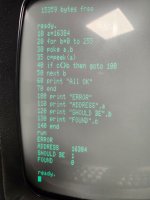
Setting aside that rabbit hole for a moment, I typed in the quick BASIC memory test that Dave suggested, and got the result below. Did I type something wrong, or did it really fail on the the very first byte of the upper 16K?


20220927_215435.jpg
 
Back
Top