My XT-alike machine (admittedly new build, but the fact it's running a V40 makes it inherently vintage-flavoured) was designed with all the RAM and ROM on a seperate expansion card.
This would be okay, except that it only has 512k + a 32k UMB at F0000. 32K of UMB isn't enough to load DOS high with USE!UMBS (seems to just freeze on boot), and 512K is whittled down to like 450k of usable low memory by the time DOS and the unimaginable luxury of a mouse driver and SETVER is loaded. I want to run GeoWorks 1.2 on it but I can see it swapping furiously when I try.
To fill the gaps, I could order an off-the-shelf 1MB card, like the Montech or Lo-Tech products, but since I'd still need the BIOS ROM somewhere, that wastes a slot just to keep the ROM around. Why not a single board with the full megabyte PLUS a ROM socket at F8000?
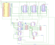
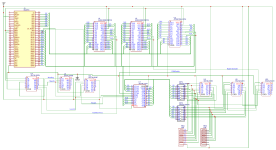
Here's the schematic I've been working on so far:
* Use two Alliance AS6C4008s to cover 1Mb
* I can do /SMEMW NAND /SMEMR to get a signal that's high when memory is accessed (either read or write), and AND that with AEN to get to "memory ready"-- we have a good address and actually want to interact with memory.
* I can invert A19 to decide if we're in the low 512K.
* Do "Memory Ready" NAND /A19 to decide if we should chip-select/output-enable the "low 512k " chip. The chip-select and output enable are active low, so it should only come on with both conditions true.
* Use inverted "Memory ready" and /A19 as the two active-low enable signals on a 74154 4-to-16 Multiplexer.
* Use A15-A18 as the four select bits for the 74154. This will drop one of 16 output lines low, corresponding to the 32k range desired.
Here's where it gets interesting:
* The 16th output line can be wired directly to the 32k ROM's chip-select and output-enable.
* The other 15 lines are put through jumpers or DIP switches.
The 15 outputs are AND'd back together with three 7421s, and a +5 (to finish off the last input on the 7421) so if any of them are low, it pushes a signal down that we can use as chip-select/output-enable the "Upper 512K RAM" chip.
This gives 15 user-controllable sections between 504k and 996k that can have the RAM deactivated to fit around peripherals and addon BIOSes.
This all seems to make sense to me in theory, but I suspect there's a lot of knowledge of physical-level behaviour I don't know about. My previous PCB-design projects have been keyboards with canned controllers, so pretty much laying out a fairly naive matrix with negligible timing requirements.
I'm worried about a few things:
1. Performance. The 74LS154 quotes a propagation delay of 35ns, and then you're also going through a couple additional gate delays. Is this likely to push things to slowly for zero-wait-state 8MHz operation?
2. Pullup resistors. Never tried it before-- am I speccing it correctly? see a lot of vague handwavy "anything from 10k to 100k will work" discussions, not sure if that's performance critical, but I suspect it varies by logic family.
3. Anything I missed from an analogue, timing, or missing signals standpoint. I know the spec needs decoupling caps on each chip, but I had a hard time getting either Kicad or EasyEDA to place them sensibly, they always want to tie them back into *some* 5V and ground pin, nowhere near the part being decoupled, so I figure I'll add those in once the schematic is finalized and the footprints are on the PCB.
I know some people have done RAM expansion circuits for XT-class machines here, so hopefully they can see what incredibly ignorant and stupid choices I've made.
[Edit] ... Yes, U5 is missing its ground connection. Somehow I lost the EasyEDA configuration and reverted to a saved copy. I could also eliminate the 7408 entirely by using the second 4-way AND gate in U10, and feeing in +5 for two inputs., but this is hard enough to read as-is.")
This would be okay, except that it only has 512k + a 32k UMB at F0000. 32K of UMB isn't enough to load DOS high with USE!UMBS (seems to just freeze on boot), and 512K is whittled down to like 450k of usable low memory by the time DOS and the unimaginable luxury of a mouse driver and SETVER is loaded. I want to run GeoWorks 1.2 on it but I can see it swapping furiously when I try.
To fill the gaps, I could order an off-the-shelf 1MB card, like the Montech or Lo-Tech products, but since I'd still need the BIOS ROM somewhere, that wastes a slot just to keep the ROM around. Why not a single board with the full megabyte PLUS a ROM socket at F8000?
Here's the schematic I've been working on so far:
* Use two Alliance AS6C4008s to cover 1Mb
* I can do /SMEMW NAND /SMEMR to get a signal that's high when memory is accessed (either read or write), and AND that with AEN to get to "memory ready"-- we have a good address and actually want to interact with memory.
* I can invert A19 to decide if we're in the low 512K.
* Do "Memory Ready" NAND /A19 to decide if we should chip-select/output-enable the "low 512k " chip. The chip-select and output enable are active low, so it should only come on with both conditions true.
* Use inverted "Memory ready" and /A19 as the two active-low enable signals on a 74154 4-to-16 Multiplexer.
* Use A15-A18 as the four select bits for the 74154. This will drop one of 16 output lines low, corresponding to the 32k range desired.
Here's where it gets interesting:
* The 16th output line can be wired directly to the 32k ROM's chip-select and output-enable.
* The other 15 lines are put through jumpers or DIP switches.
The 15 outputs are AND'd back together with three 7421s, and a +5 (to finish off the last input on the 7421) so if any of them are low, it pushes a signal down that we can use as chip-select/output-enable the "Upper 512K RAM" chip.
This gives 15 user-controllable sections between 504k and 996k that can have the RAM deactivated to fit around peripherals and addon BIOSes.
This all seems to make sense to me in theory, but I suspect there's a lot of knowledge of physical-level behaviour I don't know about. My previous PCB-design projects have been keyboards with canned controllers, so pretty much laying out a fairly naive matrix with negligible timing requirements.
I'm worried about a few things:
1. Performance. The 74LS154 quotes a propagation delay of 35ns, and then you're also going through a couple additional gate delays. Is this likely to push things to slowly for zero-wait-state 8MHz operation?
2. Pullup resistors. Never tried it before-- am I speccing it correctly? see a lot of vague handwavy "anything from 10k to 100k will work" discussions, not sure if that's performance critical, but I suspect it varies by logic family.
3. Anything I missed from an analogue, timing, or missing signals standpoint. I know the spec needs decoupling caps on each chip, but I had a hard time getting either Kicad or EasyEDA to place them sensibly, they always want to tie them back into *some* 5V and ground pin, nowhere near the part being decoupled, so I figure I'll add those in once the schematic is finalized and the footprints are on the PCB.
I know some people have done RAM expansion circuits for XT-class machines here, so hopefully they can see what incredibly ignorant and stupid choices I've made.
[Edit] ... Yes, U5 is missing its ground connection. Somehow I lost the EasyEDA configuration and reverted to a saved copy. I could also eliminate the 7408 entirely by using the second 4-way AND gate in U10, and feeing in +5 for two inputs., but this is hard enough to read as-is.
Attachments
Last edited: