super-sama
Experienced Member
I'm putting this out there as a general call-out to anyone interested in a challenge. simply put, there are a lot of NOS TI486SXLC2-G50 chips that are available on eBay. (listing provided as example, there are others with more available for up to $18 shipped in some cases.) These are 3.3v, with 5v-tolerant I/O. These can't be used in a 5v system without a regulator and I don't know what else. some interposer boards with such a CPU on them have a couple extra chips probably for compatibility reasons, but what they do is beyond the scope of my knowledge.
386SX interposers in general are getting very scarce and people are wanting stupid amounts of money for the ones that are left, especially the ones meant for IBM PS/2 systems like the 50 and 60 models. All of the IBM boards I've seen use the FPU socket for the upgrade, and this may also be because they were originally designed for 286 systems, but I can't tell. From what I understand, these work in a different way to the normal interposer boards out there and are only specifically compatible with IBM PS/2 systems and do not work on any others, so this would not be the target audience of the proposed board.
the proposal is to develop and make available a board which either sockets atop a BQFP100 386SX or compatible clone, or uses the PLCC-68 FPU socket to disable the onboard 386SX and take over, with 5v to 3.3v voltage regulation and whatever else is necessary to get these properly enumerated at boot time.
The datasheet for the TI486 chips are here: http://bitsavers.informatik.uni-stuttgart.de/components/ti/TI486/1994_TI486SXLC_and_TI486SXL_Microprocessors_Reference_Guide.pdf
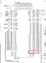
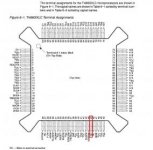
what the PDF doesn't go into too much detail about is the VCC5 pin, which is present on the 144-pin QFP package chips, meant to provide 5v for I/O. According to another PDF here: https://www.versalogic.com/products/manuals/M4863.pdf the schematic for the SXLC2 calls for pin #45 to be attached to +5? and yet all the TI official PDF says is that pin #45 on the QFP100 package of other models of the TI486 are all NC, so this is likely *just* an SXLC2-G50 feature since it is a 3.3v chip with 5v-tolerant I/O.
These two images here explain where it is in the two PDFs of the conflicting information, but the TI PDF is older and the SXLC2 was still listed as "advance information" in this. the 144-pin QFP has the pin for I/O voltage listed however.


now, I may be 100% in the wrong here, but is something like this doable? I'm almost certain it'd become a multi-layer board, and it likely will not work for everyone since these chips require a utility to flip a register to activate clock doubling and not all boards like that. likewise they also need a utility to enable the 8K of cache on the chip to get the extra speed gains. This would be for people with a 33-50MHz crystal already on their board, a 386SX-16/20/25, and an optional 387SX at 16-25MHz. however I can also see it being a good way to get say, an am386sx-40 onto a board too, with less hassle.
the only problem I see being faced is the connection to the PLCC-68 socket with pins, or finding a snap-on socket for a BFQP-100 chip. the former seems doable, but the latter seems a bit more exotic.
386SX interposers in general are getting very scarce and people are wanting stupid amounts of money for the ones that are left, especially the ones meant for IBM PS/2 systems like the 50 and 60 models. All of the IBM boards I've seen use the FPU socket for the upgrade, and this may also be because they were originally designed for 286 systems, but I can't tell. From what I understand, these work in a different way to the normal interposer boards out there and are only specifically compatible with IBM PS/2 systems and do not work on any others, so this would not be the target audience of the proposed board.
the proposal is to develop and make available a board which either sockets atop a BQFP100 386SX or compatible clone, or uses the PLCC-68 FPU socket to disable the onboard 386SX and take over, with 5v to 3.3v voltage regulation and whatever else is necessary to get these properly enumerated at boot time.
The datasheet for the TI486 chips are here: http://bitsavers.informatik.uni-stuttgart.de/components/ti/TI486/1994_TI486SXLC_and_TI486SXL_Microprocessors_Reference_Guide.pdf
what the PDF doesn't go into too much detail about is the VCC5 pin, which is present on the 144-pin QFP package chips, meant to provide 5v for I/O. According to another PDF here: https://www.versalogic.com/products/manuals/M4863.pdf the schematic for the SXLC2 calls for pin #45 to be attached to +5? and yet all the TI official PDF says is that pin #45 on the QFP100 package of other models of the TI486 are all NC, so this is likely *just* an SXLC2-G50 feature since it is a 3.3v chip with 5v-tolerant I/O.
These two images here explain where it is in the two PDFs of the conflicting information, but the TI PDF is older and the SXLC2 was still listed as "advance information" in this. the 144-pin QFP has the pin for I/O voltage listed however.


now, I may be 100% in the wrong here, but is something like this doable? I'm almost certain it'd become a multi-layer board, and it likely will not work for everyone since these chips require a utility to flip a register to activate clock doubling and not all boards like that. likewise they also need a utility to enable the 8K of cache on the chip to get the extra speed gains. This would be for people with a 33-50MHz crystal already on their board, a 386SX-16/20/25, and an optional 387SX at 16-25MHz. however I can also see it being a good way to get say, an am386sx-40 onto a board too, with less hassle.
the only problem I see being faced is the connection to the PLCC-68 socket with pins, or finding a snap-on socket for a BFQP-100 chip. the former seems doable, but the latter seems a bit more exotic.
