• Please review our updated Terms and Rules here

Question about QBus PCB design

jplr

Experienced Member
Joined
Sep 3, 2022
Messages
153
Location
Brittany/France
Dear all,
I never used Kicad or any other PCB design tool before today, so I am sorry for the dumb things I will write in this post.
My goal would be to make a poor man QBus backplane with Aliexpress connectors (for the cost in EU) and a PCB backplane.
At first I thought that I could modify the beautiful omnibus design from GWiley, but alas in a few hours I understood that this goal and needed capabilities are well above my head.
I tried something different, I used S100 Gerger files, after all they have the good pitch between holes (they do isn't?) 0.125" and they have too much connector pins, so it it possible to cut them and add a small piece of plastic at the end (as explained in the thread of omnibus PCB).
Yet my Kicad-fu didn't improved much in the last hour, so if some kind soul would look at my attempt in included file and give me some suggestions, it would be fantastic!
I think the PCB size is missing and the drill files are incorrect but I have no idea how to correct that.
Jean-Pierre
 

Attachments

  • jplr2.zip
    73.8 KB · Views: 3
Thanks for reading.
I think a better trial is the one in included file. Size is now OK and drills list is included.
Yet I just saw that the connectors at board's end are missing on one side. I may also add later the circuitry for power OK.
 

Attachments

  • jplr4.zip
    44.9 KB · Views: 8
Thanks for reading.
I think a better trial is the one in included file. Size is now OK and drills list is included.
Yet I just saw that the connectors at board's end are missing on one side. I may also add later the circuitry for power OK.
I like @daver2's recommendation to start small and build up to a larger design, but you'll also learn a lot by just going for it. If this is your first PCB it's almost certain you'll learn many things while debugging the boards to improve in a version 2 of the design.

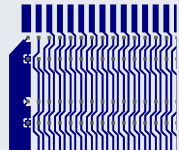
I know very little about QBUS but Imported the zip file into the JLCPCB online Gerber viewer to take a look. It complained about a few things, so I'm not certain if what I was viewing is what you intended. Here's a snippet of the upper left corner.
1675179354440.png
* Looks like a good overall approach. Nice methodical weave of signals through the pins, and signals are on the bottom side so you can see the traces.
* I would add a ground plane on the top side to minimize inductance and resistance in the ground between slots.
* It seems like there should be additional ground signals on pins in the middle of each slot. Connect those to the ground plane using thermal reliefs.
* Trace thickness on the existing thermal reliefs is a bit large for my taste. Makes it difficult to solder these pins. The distance from the pin pad to the plane is very short so the thermal relief can be thin. This helps to increase thermal resistance but electrical impedance (L+R) is still quite low.
* The Gerber viewer complained about this board not having a board outline, but maybe that's my viewer problem.
* Many of the edge-connector pins seem to not have pads, and there's an "X" on most of the pins. Not sure what that means. Again, might be an issue with my Gerber viewer? I'm referring to the board slot edge connectors, not the connector at the top in the pasted image. If you click on the thumbnail image then the crosses or X's are visible. Definitely want pads and plated-through holes for a good solder connection and solid mechanical support. Connectors will get some mechanical stress while inserting and removing boards.
* To get the weave exactly identical on every signal and every slot (not required but has a nice look) a trick is to route one trace, then copy it down to other slots, then copy those traces across the backplane. This may require some Kicad trickery to change the signal name on the copy-pasted traces. I don't use Kicad so I can't comment on the mechanics of it.
* Curious about the method for power to attach to the backplane? That's important for good power distribution to minimize voltage drop. I wish I knew QBUS better to help with this.
 
Back
Top