• Please review our updated Terms and Rules here

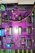
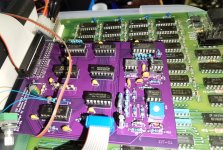
Reproduction Osborne 1 DD upgrade card

Perfect! I imagine write should be much easier to get working as the circuit is much simpler than the read section.

While the iron is hot, what did you substitute, and was it from the Sam's, official or my schematics? I may just end up updating the schematics to suit, or at least note them in.

The official schematics is in one of the two service manuals floating around, around 2/3rds in.
 
I got the values from the datasheet in the service guide edition 2. The schematics ( two pages )

From memory I think I substituted R9 and R10 - either that or it was R6 and R8. I only had close values. I'll check later with a microscope to see what I put in. Just two resistors wrong... And it was a 9v1 zener and a 180 Ohm to the 5v1 and I think a 120 Ohm to the 9v1. I needed a bit more current than the original values gave - around 10 mA more in total.

And the extra trim at the end of R2 to get the pulse to exactly 400ns. center to center.

I'll get some pics in the morning and post them with closeups of resistor colours.

I just used ceramic caps and yellow 0.1 decoupling.

David
 
I just rechecked, and of the critical change I made to the PCB;

Filter caps were whatever I could find. Mostly 0.1uF... And electros that fit. Also, a 7438N is important. I've heard of these types of projects failing if a LS is used. And all the chips came from Aliexpress.

=R2 in my case needed to be 11.1K, rather than 10K to get the right pulse width - likely because I used a cheap ceramic cap instead of a highly accurate one, so it was out by around 10%
=R3 150r - I just needed a little more power to bring the zener up to voltage for 5.1
=R11 120r - I couldn't find the 180s or 150s when I was looking. But it works, so I left it there, also it's the 9v1 zener for me rather than the 8v7 so the drop is no as much.
=R6 10K instead of 11K - because I couldn't find an 11K at the time.
=R8 15K instead of 16K - because I couldn't find a 16K at the time, and R6 was 10K, so I went with a smaller resistor.
=D3 - 9V1 Zener because I couldnt find a 8V7.

That was it. The rest was out of tolerance, but values were correct.

For me, the process was get the read pulse width correct, then I put the CRO on pin 7 of U9, and found that while adjusting the pot, it would snap to 1MHz at times, so I picked the middle of this "sweet spot" and left the pot there.

Once I did that, a disk loaded up just fine. I still have to replace the pot at R2 with a 1K1 resistor, or thereabouts... I might even go 1K2. The pulse is a little on the short side and the rise time slower than I would prefer.

David
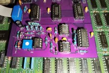
IMG_20230509_061427.jpgIMG_20230509_063245.jpgIMG_20230509_063259.jpg
 
I checked through my build once more, this time checking every component against the official schematics, and realised I'd put a 47nF cap in C3, instead of 47pF. I swapped it out, and no dice. I can get U9 up to 981 MHz, but no further.
I'll check voltages again later, but I may end up just doing a digikey order with the exact correct parts if I still can't get my one to work.

From what I can tell the only deviations from the official schematics are
C3 & C4: 47pf 50V 5% (should be 1%)
C17: 10nf 50V 20% (should be 47nf 6v 20%)

D1: 1N4733 (1N5231B)
D2: 1N4730 (1N5228B)
D3: 1N4733 + 1N4729 (1N5238)

R1 & R10 are with 1% parts that fit within the tolerance of the specified parts
R12: 4.7K 5% (1%)
U2: 74LS01 (7438, rotated and VCC / GND fixed)
U5,U6: 74HC107 (74LS107)

C3 & C4 is a good candidate
C17 doubtful

D1/D3 Doubtful as the voltages were ok
D2 is a maybe

R12 I don't suspect because it's on the trimmer, but it's also probably the easiest to test / fix

U2 maybe
U5/U6 doubt as the voltage levels should only be an issue at the input, and it'd got input from digital stuff.

I'm still super happy the design works, but immensely frustrated that I've messed mine up!
 
980KHz is higher than mine free-runs at... So should be OK. I believe it's supposed to be a bit lower than 1MHz, but I don't know how much lower. Mine is around 960MHz IIRC. Getting the trim-pot set correctly requires an oscilloscope. You will only get 1 MHz when there's an input signal on the RDATA line from the Floppy Disk.

If you set up the Gotek so it can boot an image, and turn the POT until the W comes up on the GOTEK, then let it rewrite the first track, and then adjust it back until Pin 7 of U9 locks to 1 MHz should be enough to get it working from what you describe.

C17? I don't remember a C17... I thought C16 was the last... Did I miss one? Oh, c17 is the electrolytic. I got 100uF in C17... Do you mean C14?

If your data pulse width is correct, and your RX clock locks to 1MHz when there's a signal present from the drive, then you should be able to switch from the calibration image to a valid boot disk on the Gotek and boot. I can't think of any way to know that it's syncing properly other than using a scope and adjusting it live.

David

Oh, and Nice work on the circuit design... Yes, it did work first time. It's just difficult to get the two critical timing elements spot-on.
 
Last edited:
Yeah, C17 is the electrolytic on the side, so I'm not too phased about that.

After studying the schematics, and playing around a bit, I see the "snapping on" behaviour you mentioned.

U7 and downstream of that is responsible for finding a bias to nudge the 1MHz signal from U8,9,10 up and down to match the variable frequency that MFM can give.

R5 looks to bias the "nudge" fed into U9.

From what I can tell, my 1MHz section still isn't getting up to the right frequency.

On my board, with R5 all the way to one end, I get 962KHz without data coming in, and about 980KHz with a signal.

The voltage jump at U9/3 is about .2 volts in that situation.
When I wind R5 down a bit to somewhere in the middle, the voltage jump and presumably the frequency jump is bigger.

I'm reading this to mean that U7 is running out of puff to nudge U8,9,10 high enough, so U8,9,10 still aren't where they need to be.

This block is
D2 (on the input)
U8,9,10
R9,10
C14
RN5

5VA (5.1V)
VDA (8.7V)

The only things different at all from the schematics is D2, R10 (3.01K 1% vs 3K 1%) and maybe the rails.

Narrowing it down at least.
 
I am running 9.1v instead of 8.7v - That might nudge it slightly my way... But I get the "lock" around the middle of the range with the potentiometer. It might come down to chip selection or something strange like that. There's a lot of variable we're not sure about, but I'm pretty certain it comes down to the sync and the timing.

Just a question on the data- are you running normal boot sector ? And did you manage to reproduce the "write" effect with the pot fully clockwise? It was when reading that track back by trying to boot the corrupted image it created that I was able to dial in the sync... But as you say, it's getting closer... Maybe adjusting the resistors either side of the potentiometer will provide enough range? I have no idea why it writes when the pot is fully turned. That makes no sense to me at all. I am guessing there's something in the FDC chip that triggers when the sync collapses and write comes on.

I'll try populating the second PCB the same as the first, and see what I get as a result... If I get the same outcome with the same process, that will add some further data to the puzzle.

I am hoping to get my new Osborne 1's in early next week which will give me a permanent motherboard to experiment with without having to take a working machine apart to experiment. Assuming it works, that is, otherwise I will have the repair task ahead of me first - :) My new Goteks arrived, and I ordered more resistors from Amazon so I can get a better selection. I think the tolerances aren't critical for most of the components, but I'm guessing a bit about which ones matter.

David
 
No, I haven't gotten the Gotek into write mode yet, but that may be because I've been running the upgrade card in "passthrough mode" (without the card's RDCLK and RDDATA, but DDEN pulled low). I think I tried much earlier today to no avail. that behaviour being some kind of controller shenanigans would be the most reasonable explanation though.

When you say pot "fully clockwise", does that mean it's "short" to R12 (i.e. pulling up) or short to R4? Full clockwise for me is short to R12. I do notice that short to R4 the clock completely vanishes, so it wouldn't surprise me if we're breaking something's assumptions.

I've been booting the system with the SD diagnostics disk, entering the disk confidence test, getting it to constantly read the gotek, then switching the gotek to a DD image.

Measuring my "8V7" with my nice Rigol scope shows that it's actually "8V0", when my other scope was saying "8V4".

My R5 should also get to ~3.4, but only gets to 2.4, but that partially looks like there's current being sinked somewhere it shouldn't.
 
Okay I suspect D2 is *part* of my problem.
8.7 or 9.1 on VDA (even making sure it's not being regulated down) doesn't change anything, so it's not the op-amp limiting due to it's supply.
With U5 & U7 removed, I get the same voltages at R5/2, and R7/D2 as with them added back in. If D2 is meant to be 3.9V, I *thought* that the maximum the divider can output of 3.4 would be fine, but it always sticks at 2.1.

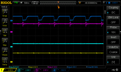
This is with R5 all the way to R12:
1683649137205.png
Ch1 is the output of the pot
Ch2 is the output of U7
Ch3 is R7 / D2 / U9/3
Ch4 is U9/7

Can you confirm that this looks right, and the measurements are about right? I'm hoping that the pot output is low (because of D2?) and that's dragging the rest of it down.

Pot output is 2.32V
U7 output is 0.827V
U9/3 input is 2.10V with spikes matching the frequency output
U9/7 output is 961kHz.
All four of these measurements react to the trimmer in the same way, so they're the highest I'm able to measure. the 5V rail seems to be pretty stable at 5.1 or 5.2V.

Thanks again for the help!
 

A short video while booting - showing how it switches from the freerunning frequency to the data rate frequency, then back to the free running frequency at the end.
 
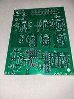
Are gerbers for this project and the latest revision of the board available anywhere? I wouldn't mind building one myself and possibly assist with its development. Thanks!
 
Are gerbers for this project and the latest revision of the board available anywhere? I wouldn't mind building one myself and possibly assist with its development. Thanks!
Heya!

There's been no further development as I've got other projects I've been working and spending money on, and the difficulty sourcing the exact right parts.

The kicad files I used to generate the gerbers for the board that cj7hawk and I have assembled are here: https://gitlab.com/NRoach44/occ1-dd-upgrade

If you want the gerbers I have a good feeling they should be around somewhere, and can get them if you need.

To tl;dr the thread, cj7hawk has managed to get his to work fine, but mine doesn't want to get it's frequency up high enough to "lock on" to the clock coming from the drive. He was closer with his parts list than I was, so that's probably why.

Once I ~eventually get around to getting the exact right parts and verifying it for myself, I'll re-spin with a shugart / IBM interface and power header.

If you're able to get it to work, it'd be helpful to get the list of substitutions you made (if any). If we can make a list of suitable replacements it'll be easier to make.
 
Thanks for the info @NRoach44! I'll be happy to report back once I get a board built and assembled. Keep us posted if you get time to 'dive into the pool' again!
 
As was mentioned, NRoach44's circuit had no faults that I found, but component selection and substitution is a bit problematic where some of the timing is concerned. The Osborne DD adapter is a bit tight on timing, which is not great since there should be no issues with going from SD to DD, it's just the way they did it with analog delays!... It could be worth adding in some small trim pots if you are adjusting the circuit so as to fine-tune the critical resistors up on the top left of the PCB ( you can see where I was experimenting with putting some external POTs on the PCB )- But if you get relatively tight tolerance components it should just work from assembly.
 
Do you have the schematics? They define the component tolerances of the two brown caps and the main two resistors on that diagram.

The problems arise when substitution of either the chip type or passive components occur due to sourcing challenges. Otherwise it should be a case of assemble and operate.
 
Please tell me that's one you prepared beforehand and not something you just whipped up over the past 24 hours while the discussion has been occuring?

Anyway, the difference between that and NRoach44's version is that This version will fit if the 80 column adapter is installed, and it may still have the errors that NRoach44's version corrected. ( See the extra resistor, and may be some cut lines IIRC ).

In populating, trust the schematics over the PCB.

Regards
David
Well I did it in just 6 hours and ran the boards on my super duper machine. Really this was done a long time ago with another fellow. This is a working board.
 
Back
Top