gatewayrepairs1985
Experienced Member
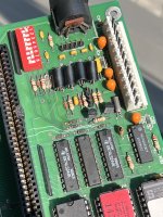
Hi all,
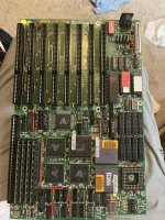
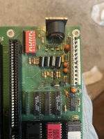
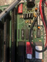
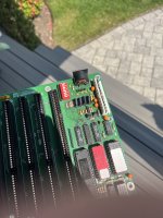
Hoping you are well. I really want to get this 33 mHz Micronics motherboard working again. When I got it, the VARTA battery had leaked, and there was corrosion surrounding it. I let the corroded part of the board sit in vinegar, then rinsed with warm water and let it dry. I still get no luck, (board powers on, no activity with POST card inserted). I have confirmed the BIOS chips are good. Here is some more info on the board:
 theretroweb.com
I have photos attached of what the board looks like right now. I have a multimeter but no experience using it. I have some experience soldering and can desolder/solder things if necessary. How should I go about getting this board to POST again? Any advice from anyone would be greatly appreciated!
Thanks so much!
Shawn
Hoping you are well. I really want to get this 33 mHz Micronics motherboard working again. When I got it, the VARTA battery had leaked, and there was corrosion surrounding it. I let the corroded part of the board sit in vinegar, then rinsed with warm water and let it dry. I still get no luck, (board powers on, no activity with POST card inserted). I have confirmed the BIOS chips are good. Here is some more info on the board:
Micronics 80386 SMT ASIC, 386 ASIC CACHE VER. 4.0 (09-00035-xx/09-00066-xx)
Micronics 80386 SMT ASIC, 386 ASIC CACHE VER. 4.0 (09-00035-xx/09-00066-xx) is a motherboard based on the Micronics MIC 361/362/363 (ISA 3/486) chipset. Get specs, BIOS, documentation and more!
theretroweb.com
I have photos attached of what the board looks like right now. I have a multimeter but no experience using it. I have some experience soldering and can desolder/solder things if necessary. How should I go about getting this board to POST again? Any advice from anyone would be greatly appreciated!
Thanks so much!
Shawn