• Please review our updated Terms and Rules here

Superbrain/Elston monitor

guilfordbob

New Member
Joined
Mar 7, 2024
Messages
7
Hi folks,
I'm working on three Superbrain computers for a nearby computer museum. (gratis). One is now working fine, two still need a lot of help, this is about one of them.
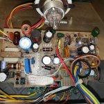
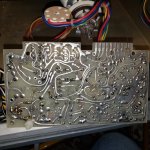
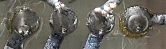
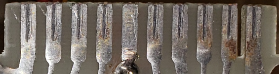
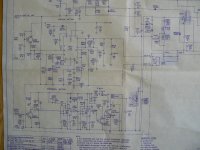
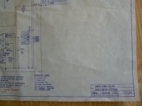
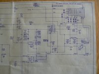
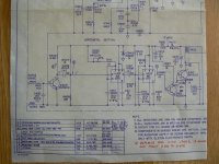
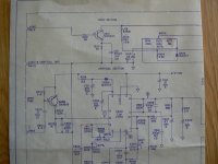
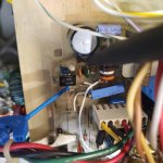
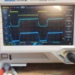
For starters, the monitor board does not seem to match the monitor schematics I've found online. Pix of the boards attached. At first the screen was dark, I replaced a bad tantalum and fuse. Still dark. I replaced the the HOT driver (pre transformer that drives the HOT) because the collector was not pulling down completely to ground. It doesn't look much better on the scope, but at least I now have something on the screen. BTW, the screen has a bad cataract, but I won't bother to work on that if I can't get the video board working.
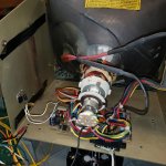
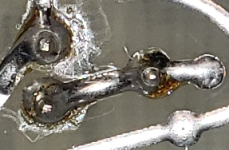
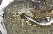
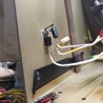
The HOT has been removed from the board, and a transistor that may or may not be the correct one has been mounted to the chassis with an added diode and cap. Also, the red lead to the pix is not going to the board marked R, but rather to the junction of two resistors that have been put across an existing(?) cap to the left of where the wire came from. However, my favorite 'mod' is the steel file taped to the side of the chassis. (the machine was a donation, maybe it came from a prison!)
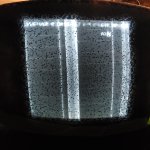
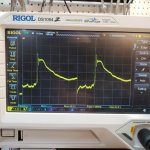
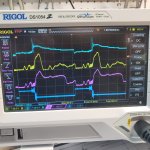
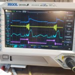
Now I have a raster of sorts. Not terribly bright, and the H-sweep is a mess. You can see some messy text at the top that is telling me to insert a disk in drive A, and below that on the right side of the screen is the CPM 'A>' prompt.
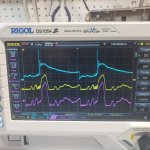
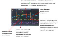
The waveform is the collector of the HOT driver. I think I've rambled long enough. Any insight is appreciated.
 

Attachments

  • 20240502_181240.jpg
    20240502_181240.jpg
    2.7 MB · Views: 17
  • 20240417_173558.jpg
    20240417_173558.jpg
    3.1 MB · Views: 15
  • 20240417_173729.jpg
    20240417_173729.jpg
    3.2 MB · Views: 15
  • 20240417_173742.jpg
    20240417_173742.jpg
    3.6 MB · Views: 17
  • 20240502_152955.jpg
    20240502_152955.jpg
    2.3 MB · Views: 17
Three things on the PCB side of the Elston Circuit Board look suspect.

1. There are solder Rings around several Pins that are soldered to the PCB Pads.
Typically, a Ring around a Pins means a bad solder Joint. One of these is a 4 Pin Plug
to some remote connection. All Solder connections need to be verified with a magnifying
device. I typically use ONLY Kesters Rosin Core Solder, and extra flux as needed. Some
of the soldering on this PCB needs re-flowed.
Photo's Rings-Around-Pins-1 & Rings-Around-Pins-2 show some of these suspect solder joints.

2. The Connector has all the PCB pads marked (used) except for one. Is this PIN actually
used and the connector and is not making contact, or is this Connector Pin unused?
Photo One-Pin-unused shows this unused connection.

3. The Photo No-PCB-pad shown a connection on one side of the PCB, and since
a Copper through hole rivet wasn't inserted through the PCB to repair the connections
on BOTH sides of the PCB, you need to make sure that the PCB trace(s) on the other side
of the PCB are connected the Lead that is sticking through the PCB.
Photo NO-PCB-Pad shown this suspect pad.

I have a PDF Document named Elston_DM30_DM40.pdf (may have been extracted from SuperBrain Tech Manual)
if you do not have it. Spot checking 4 Parts, it seems to be close to what you might need. Let me know if you need
this PDF for reference.


Larry
 

Attachments

  • Rings-around-pins-1.png
    Rings-around-pins-1.png
    101 KB · Views: 5
  • Rings-around-pins-2.png
    Rings-around-pins-2.png
    59.9 KB · Views: 5
  • One-Pin-unused.png
    One-Pin-unused.png
    310.1 KB · Views: 4
  • No-PCB-Pad.png
    No-PCB-Pad.png
    39 KB · Views: 4
Three things on the PCB side of the Elston Circuit Board look suspect.

1. There are solder Rings around several Pins that are soldered to the PCB Pads.
Typically, a Ring around a Pins means a bad solder Joint. One of these is a 4 Pin Plug
to some remote connection. All Solder connections need to be verified with a magnifying
device. I typically use ONLY Kesters Rosin Core Solder, and extra flux as needed. Some
of the soldering on this PCB needs re-flowed.
Photo's Rings-Around-Pins-1 & Rings-Around-Pins-2 show some of these suspect solder joints.

2. The Connector has all the PCB pads marked (used) except for one. Is this PIN actually
used and the connector and is not making contact, or is this Connector Pin unused?
Photo One-Pin-unused shows this unused connection.

3. The Photo No-PCB-pad shown a connection on one side of the PCB, and since
a Copper through hole rivet wasn't inserted through the PCB to repair the connections
on BOTH sides of the PCB, you need to make sure that the PCB trace(s) on the other side
of the PCB are connected the Lead that is sticking through the PCB.
Photo NO-PCB-Pad shown this suspect pad.

I have a PDF Document named Elston_DM30_DM40.pdf (may have been extracted from SuperBrain Tech Manual)
if you do not have it. Spot checking 4 Parts, it seems to be close to what you might need. Let me know if you need
this PDF for reference.


Larry
RE: the above...
1: I resoldered many points as suggested. Something has changed, as the raster isn't as large as it used to be, and possibly a little dimmer. It wasn't very bright to start with.
2: That pin (5) is not wired on any of the 3* Superbrains I have here. It's a ground. Pins 1 and 10 are also grounds, and they're wired.
3: It's making a good connection on the foil side, it's a single sided board.

I don't have a document by that name, I would like to see it when you have a chance.
Thanks.
* ...and every board is different!
 
Last edited:
Here is the Elston Document along with my Kaypro Elston Schematic and I think the DM30-120BO file
is from the Northstar Manual.


Larry
 

Attachments

  • P1020651.JPG
    P1020651.JPG
    1.9 MB · Views: 7
  • P1020650.JPG
    P1020650.JPG
    2.2 MB · Views: 6
  • P1020649.JPG
    P1020649.JPG
    1.8 MB · Views: 7
  • P1020648.JPG
    P1020648.JPG
    1.8 MB · Views: 6
  • P1020647.JPG
    P1020647.JPG
    2.1 MB · Views: 8
  • Elston-DM30-12B0-119-C31.pdf
    95.8 KB · Views: 1
  • Elston_DM30_DM40.pdf
    1.1 MB · Views: 2
I can help you fix this VDU. I have seen its schematic before.

The collector waveform of the HOT's driver transistor is not what many people expect.

One reason is that is often glossed right over and ignored in textbooks in the design of VDU's is the polarity of the driver transformer and the way the driver transistor is used to drive the HOT:

Conduction in the driver transistor turns the HOT off, not on. The reason for this is that power has to be applied to deplete the HOT's base voltage & charge very quickly to allow for flyback, where the HOT's collector must be completely cut off.

While that driver transistor is conducting for about the 1st 1/3 of the scan after flyback, on the L side of the raster, energy is being stored in the core of the driver transformer and the HOT is off, and damped current from the yoke and flyback transformer scans the L side of the raster. Then, when the driver transistor is cut off, by its drive wave, the magnetic field in the driver transformer collapses, in a controlled way because the energy is fed to the base-emitter junction of the HOT, which controls the field collapse. This B-E current flow for the HOT is sustained by this field collapse until the driver transistor switches on again at the extreme R side of the raster, and the HOT is forced off and flyback begins.

So it doesn't work the way most people imagine and these facts are often obscured because most of the time the drawers of the schematics don't bother to label the polarity of the windings on the driver transformer.

A good place to make a test is on the collector of the HOT, with a x10 probe at least for a small VDU's where the expected peak voltage is under a few hundred volts, for large ones its best to use a x100 2kV rated probe. A lot can be deduced from the waveform there on the HOT's collector.

I love that File taped in there. Maybe it was magnetized and there was a scientific reason for having it there, but it looks like a Jailbreak idea to me.
 
Top down in the scope image is the driver collector, HOT collector, and high side of the H-sweep coil. If I'm interpreting your description correctly, it appears the the HOT is behaving poorly. Thoughts?
 

Attachments

  • 20240506_113758.jpg
    20240506_113758.jpg
    2.4 MB · Views: 6
There are a number of problems.
The timing of the drive waveform to the HOT looks abnormal in that immediately after flyback the HOT Should be held off for maybe around 40% of the operating cycle and then switched on for the remaining about 60%.

But, also in the time between the flyback pulses, the collector voltage of the HOT should be close to zero. It is like this because in the first half of that time the damper diode is conducting and in the second half of that time the HOT is conducting like a saturated switch.

If during the scan time though, if insufficient energy is stored in the magnetic field of the yoke and flyback transformer, the damper diode comes out of conduction too soon and the tops of an oscillatory wave are seen. Also, the peak of the flyback voltage is reduced, this looks low too.

It suggests that something is overloading the flyback transformer, it could be shorted turns within that, or it could be a failed/leaky EHT rectifier. It looks like in this set, that is placed in the EHT Cable leading to the CRT's anode.

So check for anything that could be overloading the transformer on any of its output pins.

The duty cycle of the drive wave to the HOT is set by the second 555 timer, in conjunction with the operating frequency. The first one is merely to center the text on the screen.
 
Also if you could make a recording of pin 3 of the 555 timer that drives the H driver transistors, we could work out why the timing of the switching looks off, but that doesn't relate to the issues with the possible flyback transformer loading.

One way to eliminate the EHT diode being leaky as a cause is to disconnect the Anode of the CRT, and re-measure the HOT's collector voltage. Though if you do that it is best to place the anode cap in a thick walled glass jar to insulate it and tape it there so it can't fall out when you do the test.

You don't have to worry about discharging the Anode of the EHT in this set, it has its own 240 Meg discharge resistor (and that double wire EHT cap)

However, in this case, before concluding there is anything definitely wrong with the flyback transformer, or the EHT rectifier, I think you should fix the timing of the drive cycle first, where the HOT at the moment is being switched on very late in the cycle. I noticed when preparing the attached diagram, that the time the damper siode stays on is roughly about the same as the HOT stays in saturated conduction. So it is possible some of the events we are seeing are due to the late turn on of the HOT, and the 555 (which is wired as a monostable) to drive it has an issue with its timing components. So make the pin 3, 555 IC U402 recording with the scope first, before doing anything else.

There is also a very odd finding (unless the blue scope recording of the collector voltage of the driver transistor Q413 is accidentally inverted or the wrong place measured):

The polarity of the driver transformer for the HOT appears as though it may have had one of its windings reversed in phase. The reason is that when the collector voltage on the driver transistor is going high, the HOT should be switching on, and when the collector voltage of the driver is going low, the HOT should be turning off.

If this was the case, that somebody has tampered with the polarity of the driver transformer and accidentally reversed the winding phase of either the primary or the secondary, or fitted the wrong part, then it would also explain the timing anomaly we are seeing where the HOT is being switched on too late !

Does it look like anyone has been tampering with the driver transformer's connections or replaced the transformer in the past ?
 

Attachments

  • Cycle.jpg
    Cycle.jpg
    296.3 KB · Views: 8
Last edited:
Many thanks for detailed analysis. I'm learning a lot!
This board does appear to have been modified quite a bit. It turns out that the schematics probably matched the board better than I thought, at least originally.
I thought this board was a version with only one 555 timer. When I peeled back a S/N sticker, I see the board IS silkscreened for two. Only U402 is installed, with some added wires bypassing U401. See first image.
The HOT has been replaced with a TIP31C attached to the chassis, with diode and RIFA cap in series across the collector/emitter. The wire from the circuit board from the collector pad is connected to the junction of the two. see second image.
In the scope image I sent previously, the yellow trace that I had indicated was the HOT collector was actually the lead going to the collector pad on the circuit board (junction of the diode/cap). The actual HOT collector is somewhat different.
The third image below shows, from top down:
driver collector
HOT collector pad on the circuit board (junction of the diode/cap)
HOT collector
pin 3 of U402

I think I'll need to reverse some of these changes, but I'll wait till I hear back from you.
 

Attachments

  • 20240509_102856.jpg
    20240509_102856.jpg
    2.3 MB · Views: 5
  • 20240509_102815.jpg
    20240509_102815.jpg
    669 KB · Views: 5
  • 20240509_104232.jpg
    20240509_104232.jpg
    869.4 KB · Views: 5
With regards to those mods, they have isolated the collector with a series diode,that would slighly reduce the width. But the original HOT had the damper diode in it, so using their added diode, they would have had to add a separate damper diode on the pcb where the collector connection went. The rifa cap is to alter or increase the tuning capacitance on the flyback transformer primary, this affects the scan with and EHT and flyback time.

The collector waveform on the driver transistor is inverted, compared to what it should be. The polarity of the pulse from the 555 is correct.

The output from the 555 undergoes two stages of inversion by the time it appears on the collector of the transistor driving the driver transformer. But the waveform shows it is only inverted once.

Looking at the circuit (attached (unless somebody has modified it) the only way I think this could likely occur as a spontaneous fault, is that the pre-driver transistor, the Q401 2N3904, has failed and its emitter gone open circuit or disconnected, and signal is being coupled by its base-collector junction to the driver transistor base. Or, possibly the driver Q413 has an open emitter but a shorted base-collector, though that is not particularly likely because the drive to the transformer would be very low. In any case check those transistors and the wiring.
 

Attachments

  • Timing.jpg
    Timing.jpg
    156 KB · Views: 6
..............Scope the collector of Q401 , collector of Q413 at the same time as pin 3 of the 555 should sort it out.
 
Sadly, this board has no Q401, it doesn't appear to have a silkscreened location either. Pin 3 of the 555 goes to R468 (10K), and that connects directly to the base of Q413.
 
Sadly, this board has no Q401, it doesn't appear to have a silkscreened location either. Pin 3 of the 555 goes to R468 (10K), and that connects directly to the base of Q413.
It is a pain when the schematic doesn't match the board.

If that is the case then one of the windings on the driver transformer has somehow got reversed in phase.

At the moment, the initial recordings at least suggest the polarity of the drive to the HOT is incorrect, in that when pin 3 of the 555 is high (for its timed period) the HOT is switched on. The reason this must be the case is that when that time period finishes, the HOT comes out of conduction and the flyback peak (albeit abnormally low occurs)

In any case to double check things, can you make a recording of the collector voltage of Q413 and the the base voltage of the HOT to confirm the polarities of the transformer.

(there is other evidence too of the phase of the drive being incorrect, in that normally, the timing of the period from which the HOT is switched on is well away from the timing of the H drive or H sync pulse. The timing of the 555 then, should start close to the incoming H sync, and terminate perhaps around the 24uS to 30uS mark, after the leading edge of the H sync, the 555's timing period should not start in the middle or during the scan somewhere, which is what it is doing at the moment. This is probably why you also saw the cursor on the R side of the screen too, as the video signal coming from the computer has that only a little while after the H sync, early in the scan time)
 

Attachments

  • 20240512_125504.jpg
    20240512_125504.jpg
    2.3 MB · Views: 0
Hugo, it's working!
When I pulled the board I finally noticed that the emitter and base wires from the HOT to the circuit board were swapped.
Image, top down,
555 pin 3
Q413 collector
HOT base

I'm a bit surprised that nothing burned up in this configuration.

The image is a bit wide. I have to get a tool to fit the slug in the width coil. The other adjustments all seem to be within range.

Thank you so much for all your input. There may be questions in the not too distant future on another Superbrain, but I need to get the motherboard working first so I have some H-pulses.

Also, thanks to Larry for his comments and diagrams early in the thread.
Bob
 

Attachments

  • 20240512_165850.jpg
    20240512_165850.jpg
    2.5 MB · Views: 0
Last edited:
Hugo, it's working!
When I pulled the board I finally noticed that the emitter and base wires from the HOT to the circuit board were swapped.
Image, top down,
555 pin 3
Q413 collector
HOT base

I'm a bit surprised that nothing burned up in this configuration.

The image is a bit wide. I have to get a tool to fit the slug in the width coil. The other adjustments all seem to be within range.

Thank you so much for all your input. There may be questions in the not too distant future on another Superbrain, but I need to get the motherboard working first so I have some H-pulses.

Also, thanks to Larry for his comments and diagrams early in the thread.
Bob
It is always rewarding when circuit theory agrees with reality.

Driver transformers for the HOT, in VDU's or TV's tend to have a similar format, in that they are usually 10:1 turn's ratios or thereabouts.

The secondary winding, which drives the B-E junction of the HOT, has a low DC resistances and relatively few turns. This confuses some people who do tests on the HOT in circuit, and it shows a B-E short, and they falsely conclude the HOT is defective.

In this case though, all is explained because if you reversed those B-E feed wires to the HOT, the phase of the drive voltage to the transistor is inverted (as we concluded from the cope recordings - equivalent to reversing the phase of the secondary of the driver transformer) but due to the very low inductance and DC resistance of the secondary of the driver transformer, it does not matter that the base (rather than the emitter) of the transistor got grounded because the emitter current simply passes through that short driver transformer secondary to common.
 
The rifa cap is to alter or increase the tuning capacitance on the flyback transformer primary, this affects the scan with and EHT and flyback time.
Interesting thread....If a cap in that position affects the scan width, you might want to check it (before messing with the coil)? Cracked RIFAs are more than often out of spec
 
Back
Top