• Please review our updated Terms and Rules here

Tektronix 4054A with bicolor DVST - bright orange spot when screen dims issue

nikola-wan

Veteran Member
Joined
Mar 7, 2018
Messages
1,302
Location
Texas, USA
I have had a video issue with my 4054A since my last youtube video with my SVG image of the Back to the Future Delorean Time Machine on Nov 27 2023:


sddefault.jpg


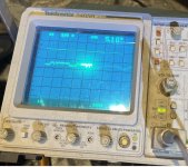
One symptom of the issue is a bright orange spot in the center of the screen after two minutes of inactivity in the program or keyboard as shown in the next picture:

4054A Checksum Test - dimmed screen bright orange middle spot.jpeg

The bright orange spot is two lines above the Diagnostic ROM text.

A second symptom is the series of dots visible under each of the text characters in the middle of the screen - but not visible on the far left and far right sides.

You might notice my Checksum test reporting U845 and U863 CRC Errors - please ignore those messages. When I rechecked the Tektronix CRCs listed in the Diagnostic ROM Pack - U845 and U863 do NOT have CRCs reported on any of the BASIC ROM versions through version 5.1, nor the A-Series version 1.3 and 1.4. I believe I need to remove those two tests as the Diagnostic ROM Pack is bank-switched into the same address 0000-3FFF ROM space as the U845 ROM and therefore cannot actually access the U845 ROM Pack when the CALL "CRC" is being executed.

I spent the last two days with my 4054A top cover removed - performing the 4054 service manual calibration test procedure with the calibration programs published in my latest Flash Drive update.

One of the calibration steps for the 4054/4054A with Option 31 bicolor DVST is to adjust CRT BIAS on the High Voltage & Z-Axis board for Option 31 display to eliminate the dot below the blinking cursor.

Here are the instructions for that step:

1704199557892.png

I was unable to get the spot below the blinking cursor to disappear in Step 6 - and the spot was visible in Step 5 on all positions of the CRT BIAS pot.

In addition - if I stopping typing or moving the cursor for two minutes - the bright orange spot in the middle of the screen appeared - and no adjustment of CRT BIAS affected that spot.

If I pressed the SHIFT key - or any other key the middle orange bright spot disappeared and the cursor appeared.

If I held down any key so it auto repeated - I observed no dot below the cursor until characters were printed near the middle, then the dot disappeared on the right side of the screen, just like the Checksum test photo above.

I have run the Diagnostic ROM Pack on the System ROM, long system memory test, Option 30 Dynamic Graphics memory test - all with no errors.

I have reseated the ribbon cables on both ends connected to the Option 30 board from the I/O board, Vector board and Display board with no change in symptoms.

I have now disconnected the Option 30 board and recabled back to the standard 4054 cabling - and still no change in symptoms.

I now believe I have a hardware issue in the CRT BIAS circuit - as this is the only mention in the calibration procedures of "dot appears in one corner of the cursor".

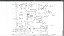
Here is the service manual page for the High Voltage & Z-Axis board for Option 31:


4054 High Voltage & Z Axis Bd for Opt31.png

CRT BIAS pot is in the bottom right corner in the Z Axis Amplifier section.

The pot slider is connected to the CRT Control Grid. Note that TP778 is the high voltage output of this board to the CRT Anode.

Here is the High Voltage Check at the beginning of the 4054 Calibration. I have NOT performed this test as I don't have a high voltage probe for my Fluke meter.

Note Step 5 below says if the high voltage is NOT between -5700V and -6300V you will have difficulty in making the Display Adjustments!

1704200886155.png

The High Voltage and Z-Axis power supply has a metal cover over the high voltage section - but there is a hole in the top of the cover and I can see the TP778 test point inside the cover.


I have ordered a Fluke 80K-40 probe to test the high voltage.
 

Attachments

  • 4054 High Voltage & Z Axis Bd for Opt31.png
    4054 High Voltage & Z Axis Bd for Opt31.png
    1.2 MB · Views: 2
Last edited:
I received my Fluke 80K-40 (useful range up to 40KV) high voltage probe and tested my Tektronix 4054A High Voltage power supply output test point today and my Fluke 89 IV True RMS Multimeter reads -6.040V which multiplied by the 1000x divider in the Fluke HV probe = -6040V.

The HV supply test point TP778 is a terminal with a small hole - so the high voltage probe tip rests inside that hole and is insulated from the metal cover by the slightly green insulating material with the round hole. So I inserted the probe into test point TP778 and then was able to leave the probe connected without touching it - and then turned on the power switch. The measurement stabilized in a couple of seconds - and the reading was steady for a minute or so to take the reading and then turn the power switch back off.

This voltage is right in the center of the -5700V to -6300V range listed on page 2-19 High Voltage Check in the calibration procedure in my previous post. BTW - the first photo shows the HV Probe safety ground clip attached to a bigger ground clip. I removed that other ground clip and associated scope probe green wire ground to make the measurement in the second photo.

This tells me I need to check out the CRT BIAS circuitry on the High Voltage power supply - as I am unable to adjust CRT BIAS to remove the "dot" underneath the blinking cursor position.

Next step will be to wait 30 minutes after power off and then remove the High Voltage power supply from my 4054A as the CRT BIAS potentiometer and surrounding components are underneath the metal cover of the HV supply.

Fluke 80K-40 HV probe on 4054A HV supply.jpeg


HV Supply at -6040V.jpeg
 
Last edited:
Ok - after the OK High Voltage check, I went through the calibration again (skipping the low voltage checks because they were ok when I checked yesterday.

First issue - High Voltage Power Supply Jumpers in wrong locations:
- My mistake, looking from the above the top of the high voltage power supply - jumper #s and pin 1 were invisible. You should NOT have to change these jumpers for Calibration. I thought they needed to change like the Anti-Burn jumper. My mistake :cry:
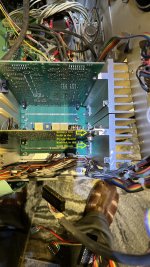
. Here is my photo of the correct HV PS jumper locations. Pin 1 on each jumper is towards the top of this photo. NOT Clear on the microfiche image. Also the calibration instructions have weird descriptions of jumper locations like middle.

HV Power Supply is easy to remove - one nut with lock washer at the top of the PS - then carefully lift off the Interconnect Board.

Interconnect board after HV Pwr Supply is removed.High Voltage power supply is plugged into the Interconnect board.jpeg

HV Power Supply (Option 31 CRT): HV Power Supply (Opt31) - Top View with cover.jpeg HW Pwr Supply (Opt31) cover removed: HV Power Supply (Opt31) - Top View with cover removed.jpeg

Cable from HV Power Supply to CRT must be removed - remove two nuts with lock washers from Metal CRT cover, then disconnect the cable from the end of the CRT.

I saw no burn marks from damaged components - so examined the jumpers and saw my bad jumper changes - YOU DON'T NEED TO CHANGE THE JUMPERS ON THE HV Pwr Supply for the calibration!

Correct jumper locations:
HV Supply Jumpers - Right.jpg Jumpers removed: pin 1 in RED and my jumper mistakes HV Supply Jumpers - Wrong.jpg

These jumpers NEVER have to change location (from the photo on the left)!

After changing the jumpers to the correct location, reinsert the HV Power Supply into the Interconnect board. Be careful that you don't bend the Interconnect board pins. The power supply is supposed to slide on the four internal black plastic spacers.


Check that all Interconnect backplane pins are straight. Ensure that Interconnect pins are straight before inserting HV PS.jpeg
Then check that every Interconnect backplane pin was inserted: Check that each pin is actually inserted into HV PS.jpeg

I then powered on the 4054 with the Anti-Burn jumper lowered on the Deflection Board and reset the Op Voltage back to 240V - which was on the calibration card on the monitor and reset CE2 to 55V and CE1 to 60 V.

I still had the issue of the Write-Thru being too bright, so I set the Coarse Write-Thru brightness to min and the Write-Thru brightness next to the Power Supply switch under the keyboard to min - and still had the original issue.

At this point I'm studying the HV PS Option 31 schematic (attached to first post in this thread) for how the Write-Thru brightness signal works in the Intensity Control Logic section. I see U615C (74LS86) feeding U616 (7410) gates through diodes to the Coarse Write-Thru R425 pot and Normal Brightness R716 pot.
 
Last edited:
I believe I found a bad 7410 on the High Voltage Power Supply board!

I was following the WRITETHRU_0 signal from the Display Controller to the High Voltage Power Supply board:

Test 1 - I put the scope lead on the High Voltage Power Supply P20 pin 10 and the signal was at 0V or 5V when the program was drawing or printing characters - looked OK!
Test 2 - I moved the scope lead to U615C output on pin 8 and the low and high voltages checked out - OK
Test 3 - I moved the scope lead to U616C pin 8 and the output is NOT GOOD - see second photo.

Checking WRITETHRU_0 on HV PS.jpg

The scope in the next photo is set for CH1 1V per division. The dotted line is on top of the 0V and the solid line is at 5.1V. The 7410 output is wiggling around 3.25V - and NOT able to go to 0V.
Since the 7410 has a high current totem-pole output - I suspect the lower transistor in this output is open circuit.


7410 WRITE_THRU output bad on HV Pwr Supply.jpg


Here is the 4054 Technical Data manual description of the Intensity Control Logic.

1704815750326.png

I marked yellow underlines on Write-Thru intensity adjustment.

My current issue is I am unable to adjust the Write-Thru intensity with the Coarse Adjustment R425 or even CRT BIAS in the output of the Z-Axis Amplifier.

I think the stuck high output of U616 gate C is enabling the BRIGHT circuit continuously - causing the display to overdrive the Write-Thru dots, lines and even show lines when the beam is moved.

I have a TI SN7410N IC ordered to replace U616.
 

Attachments

  • 7410 WRITE_THRU output bad on HV Pwr Supply.jpg
    7410 WRITE_THRU output bad on HV Pwr Supply.jpg
    465.5 KB · Views: 1
I did find an Option 31 High Voltage Power Supply component locations photo - and another copy of the schematic after the Option 10 Printer Interface.

I brightened the photo with GIMP to better show the component numbers:

4054 High Voltage & Z Axis Bd for Opt31-Component Locations-brite.png
 
While I'm waiting for my replacement 7410 IC - I have been studying the HV Power Supply schematic some more and now have questions about the Calibration procedure jumper settings for this board.

Here is the page with the jumper settings:

1704837600749.png

As I look at this schematic AND the other 4054 schematics - they show a jumper in the default position on all the schematics.

On the Option 31 High Voltage Power Supply schematic (earlier in this thread) shows the default jumper positions as follows:
  • default Z-Axis jumper J311 connecting pins 1 & 2, labeled Z0 - which matches the calibration name of the setting (but there is no inner position on the 3-pin jumper)
  • default 90/100 jumper J739 connecting the pins labeled 100 - which matches the calibration name of the setting (but there is no middle position on the 3-pin jumper)
  • default 75/93/50 jumper J411 connecting pins 3 & 4 labeled 50 - NOT 93 but I would say that 50 could be considered the outer position on that jumper
  • default for jumper J611 is connecting pins 1 & 2 labeled WT-FOCUS - NOT pins 2 & 3 which are labeled WT-DEFOCUS
  • default for jumper J512 is connecting pins 2 & 3 labeled REMOTE - NOT pins 1 & 2 which are labeled LOCAL and connected to Ground!
    • This jumper connects the Hard Copy pot under the keyboard near the Power Switch in the REMOTE position
  • default for jumper J511 is connecting pins 2 & 3 labeled REMOTE - NOT pins 1 & 2 which are labeled LOCAL and connected to Ground!
    • This jumper connects the Write-Thru pot under the keyboard next to the Power Switch in the REMOTE position
In fact the Write-Thru Intensity Adjustment step in calibration requires the front Write-Thru pot to midrange before adjusting R425 the Coarse Write-Thru port.
Same issue with the Hard Copy intensity adjustment step requiring the Hard Copy intensity pot to be midrange.

I was confused when I started the calibration - the calibration list of jumper settings had pin numbers - but there are no pin numbers visible on the board (but pin 1 on all the jumpers is a square solder pad and all the other pins are round solder pads) - and those jumpers are hard to see and hard to change as the High Voltage power supply is mounted vertically at the bottom of the 4054 enclosure with those jumpers at the bottom of the power supply.

The calibration text says to check the strap settings - it doesn't say CHANGE the strap settings.

There are two jumpers (ANTI-BURN and TEST) that DO change position during the calibration - but the text says DO NOT change any jumper while powered on and the calibration steps have you power off the 4054 before changing those two jumpers.

I believe the schematic default jumper locations are what I should change back to, when I pull the High Voltage Power Supply out to replace the 7410 U616,
 
Last edited:
I finally received my 7410 IC order (North Houston USPS changed its tracking software and delayed receipt for weeks) replaced that IC on the High Voltage Power Supply - and now have new problem, I can't see any stored (green) text :(

The 4054 Storage Board Block Diagram shows the Storage Board is responsible for driving the CRT signals for storage - with the Flood Gun Amplifier driving the flood gun anode voltage responsible for storing and erasing the persistent vectors on the CRT:

4054 Storage Board Block Diagram.jpg

The first Storage Board voltage check in the 4054 Calibration tests is that Storage Board test point TP91 (flood gun anode) is between 142.5 and 157.5 and remain constant in step 14 when erasing the screen with the PAGE key.
4054 Storage Board Straps and Test Points.jpg


When I first turn on the 4054 - the voltage on TP91 is in the correct range but then immediately drops slowly (period around 2 minutes) toward 0 volts.

Here is the page 2 of 2 Option 31 Double-Erase Storage Board schematic page with the Flood Gun Amplifier circuit:

4054 Opt 31 Double-Erase schematic pg 2of2.jpg
I suspect a capacitor may be involved in the slow voltage decay - the only one I see in this Flood Gun Amplifier circuit is C15 (0.01 uF) at the top left corner in series with R15 (10 ohm) on the input of 290V to the Storage Board.

I have checked the 290V signal at the input to the HV Power Supply board - and it is stable at that point - so I guess I will remove the Storage board. I have to remove the ROM Backpack and entire back panel of the 4054 to remove the Storage board as the metal heatsink for the power transistors is bolted to the back panel.

The parts list shows C15 is a Mallory 0.01uF ceramic capacitor 500V part number SM103Z5014R9. A quick internet search did not turn up anyone with that part number so I have to do more digging.

This Tek P/N 283-0002-00 capacitor specs are in the 1989 Tektronix Common Parts Catalog 5 Resistors and Capacitors - found on TekWiki: https://w140.com/tekwiki/images/b/b8/Tektronix_Common_Design_Parts_Resistors_and_Capacitors_Catalog_5_march_1989_ocr.pdf

.01 µF 500V -20. +80. Z5U .593 diameter P/N 283-0002-00

I found this Vishay disc capacitor that matches those specs:
https://www.mouser.com/ProductDetail/Vishay-BC-Components/D103M43Z5UL63L6R

My next step is to remove the storage board from my 4054A to do some component checking - to test my theory.
 
Last edited:
Here is my 4054A with top cover removed before Storage Board removal. The top board set has been tilted back on the hinges. The Storage Board is in the card cage at the bottom of the photo underneath the short blue ribbon cable!

Also - the entire 4054A is on a aluminum cart that I modified by lowering the rear handle bar so I can transport my 4054A to events like VCF Southwest or VCF West in our Honda Fit!

4054A with top cover removed.JPEG


I removed the Storage board from my Tektronix 4054A yesterday - the removal instructions in the service manual were NOT complete - the ROM Backpack needed to be removed first and after removing the backplate screws noted in the service manual - the backplate had two more fasteners to remove inside the chassis: one screw on top of the 5V Power Supply and one nut above the AC power inlet connector. Next two photos shows 4054A backplate before to removing the ROM Backpack and my GPIB Flash Drive with Vectrex joystick cable and after removal,

4054A backplate with ROM backpack and Flash Drive.JPEG 4054A backplate.JPEG

Note the backplate is slightly bent on the right side (second photo) above the AC power connector. I think it was previously removed - likely when this 4054 got the Option 30 Color Dynamic Graphics CRT and Option 31 Dynamic Graphics coprocessor installed - neither of which is noted on the option sticker.

Also note the massive heatsinks! From left to right: Storage Board heatsink, Deflection Amplifier heatsink, Low Voltage power supply heatsink and 5V Power Supply heatsink! The 5V AC fan above the heatsinks pushes outside air into the enclosure and there are exhaust slots in the top cover.

I believe my 'new' 4054 (I upgraded it to A-Series by swapping my A-Series upgrade kit ALU, MAS and I/O boards into this 4054 which had the Opt 30 and 31 boards) was from the Tektronix 4050 development labs - as the top cover has a hole in the left side and a second 5-inch AC fan is mounted inside - blowing more outside air over the Option 31 board (and other boards in the stack hinged above the CRT). You can also see a red two-wire cable hanging from the backpack ROM slot - this cable is routed to the Expansion Memory battery backup board with charger circuit - under the keyboard - so this 4054 also had the Expansion Memory option installed at one time.

Next two photos show screw on top of 5V Power supply and and nut above AC inlet that must be removed before the backplate can be removed:


IMG_0379.JPEG IMG_0385.JPEG

The instructions for Storage board removal indicated removing the cables from the backplate and then removing the storage board. I decided to un-cable and then remove the entire stack of ALU / MAS / I-O / Option 30 boards by pulling the two hinge pins out (after taking photos of the cables to make sure I get them correctly installed after the repair) . The other photo is with the hinged board stack removed. You can see the 5-inch AC fan that cools the Option 31 board. This fan is not in any production 4054 - but there were early problems with Option 31 cooling before they put the heatsink that you see on my Option 31 Signetics 8x300 CPU.

You can also see a Red probe with a very long flexible tip that I purchased to make the Calibration voltage measurements from the four test points at the top of the Storage board - that are under the short blue ribbon cable from the Vector board to the Display board in the card cage.

IMG_0377.JPEG IMG_0378.JPEG

Next photo is closeup of the card cage. I removed the bracket on the right side which was bolted to the Deflection Amplifier and Storage Board heatsinks.
Now I could see that the storage board heatsink had two bolts at the bottom that secured the Storage Board heatsink to the main chassis - these had to be removed in order to remove the Storage Board from the card cage. This photo also shows the four Storage Board Test points and a fifth Ground Test point.

IMG_0380.JPEG IMG_0383.JPEG

and finally I was able to remove the Storage Board for bench testing - see photo in next post. I could only post 10 photos at a time.
 

Attachments

  • IMG_0383.JPEG
    IMG_0383.JPEG
    1,016.6 KB · Views: 1
Here is the Storage Board with its massive heatsink - removed for bench testing:

Storage board removed.JPEG

I used breadboard jumper wires to connect my variable 0-100VDC power supply to the storage board to test R15 (10 ohm) and C15 (0.01uF) - starting at 5VDC and increasing slowly to 50V - and the voltage was stable.

I then moved the Fluke multimeter lead to TP1 which the Calibration Tests indicate should be 142.5 to 157.5 VDC and saw the TP1 voltage was around 25 VDC with the power supply voltage at 50V - and it was stable.

I knew I could not supply all the other voltages (+290V, +175V, +15V, -15V, +5V) for the logic and transistors in the Flood Gun Anode circuit, but I noticed that R90 (82K) was connected to +290V on one side then connected to R93 (90.9K) which was connected to ground. This explains the Calibration voltage which is approximately half of 290V, and my simple bench voltage test - which appears to reject my theory that C15 could be at fault.

I will have to put the Storage Board back into the 4054 card cage - which will supply all the above voltages to perform more tests - without the stack of main boards or Vector and Display boards.

With the Vector and Display cards removed - I will be able to probe the voltages on the back side of the Storage board - and hopefully find why the Flood Gun Anode voltage decays after 4054 power on.

IMG_0392.JPEG
 
Last edited:
I stand corrected by Bob Haas - designer of the 4052/4054 micro-coded AMD2901 ALU!

The Dynamic Graphics Coprocessor board is Option 30 - not Option 31.

The Color Enhanced Dynamic Graphics storage tube CRT is Option 31.

Bob just emailed me that he has nearly got a 4054 with Option 31 CRT repaired for exhibit at vintagetek.org museum: https://vintagetek.org/

The vintagetek.org 4054 does not have an Option 30 Dynamic Graphics coprocessor - but is currently not displaying the text or vectors at full screen.

Bob explained that the Option 31 CRT has 110 degree viewing angle vs the green 4054 CRT 90 degree viewing angle and he is trying to fix that issue.

I looked at the latest 4054/4054A schematics -03 and told Bob that a different Part Number Deflection Amplifier is shown for Option 31 (CRT) - either 672-1025-00 and 670-7454-00.

I checked my Deflection Amplifier PN - and I have 672-1025-00 - but it is a paper label - so I told Bob that it may just be a component change if vintagetek.org has the original Deflection amplifier.

Here is my out-of-focus selfie pic of my Deflection Amplifier part number label - since the Deflection Amplifier and massive heatsink are still bolted into my 4054A.

1707086077753.jpeg

Monty
 
Last edited:
I have a question for @stepleton - have you done a Calibration on your 4054A?

Right now I'm ready to check my Storage board issue with slowly dropping Flood Gun Anode voltage.

Here is a photo of the label for my CRT settings.

It indicates Storage Level 240V and CE voltages of 55 and 60 - but did not indicate whether that was CE1/CE2 or CE2/CE1.

1708260838665.png

I checked the photos of the 'your' 4054A and only found this one:

1708260917704.png

The label on this CRT indicates a Storage Level of 262V, CE1=70V and CE2=81V

According to an email from Chris - the CRT section manager at Tek for 26 years - each CRT was adjusted in the factory with slightly different settings. Chris also indicated that for the 4054 with Option 31 display they are repairing at vintagetek.org - he set the Storage Level (aka OP Level in the calibration steps) higher than the sticker as the Option 31 CRT had not been powered up in decades. I don't know if you should try that on yours.

Chris also reported their 4054 original green CRT sticker showed CE1=57 and CE2=52, which matches Storage calibration step 11 notes - but is just the opposite of the CE1 and CE2 voltages on your two Option 31 CRT! I thought my voltages were 'backwards' according to the calibration step 11 note - but now I think I may have reversed my setting of CE1 and CE2 voltages. I will bet that ALL the Option 31 CRTs all have lower CE1 than CE2!

I plan to check my Storage Board voltage plugged into the backplane without the display and vector boards - so I can access the back side of the Storage board to measure all the components in the Flood Gun Amplifier - Anode circuit including the power transistor Q85 on the heatsink.

I labeled my photo of the rear of the Storage board and made a montage with the front side component layout with an inverse grayscale (using GIMP) so I could read the component labels better - next to my rear board photo with some of the final stage of the Flood Gun circuit labeled to help with my Storage board testing - which will be from the rear of the Storage board since front access is difficult with the Deflection board in front of the Storage board.

Since I will have removed the Display board which sources the GBUSY-0 and VIEW-0 inputs to the Flood Gun Control circuit on the Storage Board, I will likely just try to jumper those backplane signals to ground on the backplane to simulate View and Erase of the screen.

Storage board rear view-perspective.jpeg
 
Last edited:
Hi! yes, we've done the calibration procedure on our machine. It doesn't seem to have helped the incomplete screen clearing issue we were seeing, which I believe may be down to poor connections to some of the CRT's flood guns. We've done a lot of tweaking of the storage level and CE voltages. We've also been in touch with Chris, and on his recommendation we've tried raising the filament voltages in order to try and burn off any contamination of the flood gun anodes. This does not appear to have solved the problem, unfortunately.

If the machine were my own, I think the next step would be to remove the CRT and inspect the electrical connections going into it.
 
I tested the Storage board plugged into the backplane - with only the Deflection Amplifier board installed in the backplane.
I removed the High Voltage power supply - and all the main logic boards had already been removed.

I went through each of the 4054 Calibration steps starting with the Storage Board Adjustments up to the section with CRT Bias Adjustments (which require you to run the calibration BASIC program for patterns on the screen).

None of the Storage Board Adjustments required any of the other boards. I did add jumper wires to the interconnect backplane connector in the Vector Board slot for GND 3 (pin 15), GBUSY-0 (pin 50), ERASE-0 (pin 44), VIEW-0 (pin 42) and DBUSY-0 (pin 43) - using the Interconnect Board Component Location diagram in the schematics manual - which had all the signal names labeled. It was easy to find the interconnect board connector pin numbers on the silkscreen after removing the Vector Board. Connecting one of those pins to GND would either reset the 200 second inactivity timer or wake up the Flood Gun Anode voltage if it was in HOLD mode.

All the Storage Board voltage and waveform tests passed. I used my Tektronix 2465B scope with on-screen digital outputs of delta-voltage, delta-time and delta-frequency readings and my Fluke 89 IV DMM for the voltage readings.
I was able to squeeze my hand between the Storage and Deflection Amplifier boards to move the Storage TEST/N jumper to TEST for the storage waveform tests. Now that jumper is back to the N (normal) position.

I set the Storage Level (OP level) to 240V, CE1 to 55V and CE2 to 60V per the calibration card on top of my CRT in my previous post.

To continue the Calibration I will now have to put all the boards and cables back and run the CRT BIAS and other tests requiring running the calibration BASIC programs for the test patterns.

My recommendation for anyone performing 4054 Calibration would be purchase the long flexible test hook - which will make reaching the four test points on the Storage Board very easy! here is the link to what I purchased:
ZIBOO ZB-T15 Flexible Test Hook Clip,Professional IC Test Hook Clip Grabbers Probe Jumper,High Voltage Flexible Test Hook Clip Insulated Quick for Multimeters, Clamp Meters and Automobile Inspection
71xGJQadqYL._SL1500_.jpg
 
This repair has taken quite a while. I don't know why my first photo in this thread didn't make me think of vector monitor "spot killer". The Tektronix 4054 manuals don't use that term.

Tektronix 4054 has an ANTIBURN circuit on the Deflection Amplifier with this quote in the 4052/4054A Technical Data manual:
"Provides Antiburn protection to prevent crt phosphor damage due to a slow moving, high intensity beam."
The "orange" spot in my first photo in this thread is in the middle of the screen - when the screen dims. That movement of the beam to the center of the screen is controlled by the HOLD circuit on the Deflection Amplifier:

"Hold mode begins (crt operation is shifted to low intensity operation) when there is no crt input for 100 seconds. HOLD-0 goes low and connects the Channel Switch to a separate set of inputs that are at ground potential. The grounded inputs prevent beam deflection and make certain that there is minimum deflection amplifier power dissipation during Hold mode. Any keyboard operation or other input will bring the circuit out of Hold mode."

So the HOLD circuit when asserted moves the beam to the center of the screen - that is where the orange spot appears! I believe the reason it is orange and not green is due to the cursor blink (refresh or write-thru mode) continues when the screen dims. Certainly the beam is not moving at that point!

Here is the description of the Deflection Amplifier board in the Technical Data Manual.

1708517164305.png

I believe the "fifth" function would have been the Antiburn circuit - but tragically there is no further mention of this circuit in the Technical Data Manual. :(

The Deflection Amplifier schematic 2 of 2 is full of the Antiburn circuit:

There is this description for the ANTIBURN signal in the 4054/4054A Parts and Schematics manual:

1708517521562.png

Here is the second page of the Deflection Amplifier schematic with the ANTIBURN circuitry - for the Option 31 Color Dynamic Graphics CRT that I have:

1708517700009.png

The terms LA and SA are "Long Axis = X" and "Short Axis = Y" deflection. SLU = Slew. So the SA & LA ANTIBURN Sensors and the SLU Sensor outputs are summed at the U291 op-amp to generate the positive true ANTIBURN output. The bottom circuit overrides the ANTIBURN when Z AXIS positive true signal indicates a vector is being drawn (maybe - need to check this circuit too).

I had been trying to learn and use the LTspice program to model the High Voltage Power Supply - Intensity Control Logic at the bottom of the schematic in my first post in this thread. ANTIBURN is the bottom signal in that schematic and appears to modify the analog voltage to the Z AXIS Amplifier on that schematic.

Here is the beginning of my LTspice model. As I looked at the HV Power Supply Intensity Control Logic - I backtracked the source of the ANTIBURN signal to the Defection Amplifier and then had an AH-HA moment when I realized that the ANTIBURN logic was likely causing the issue of the visibility of the orange hot spot in the center of the screen!

1708518599548.png

1708524431747.png

Here is the LTspice run of the current model - only showing the PULSE waveforms for each of the possible input signals to the circuit. The circuit diagram is from the Deflection Amplifier summing op-amp - but since its output is a logic output of close to 5V asserted or close to 0V if off - I really don't need to model it until I'm modeling the Deflection Amplifier ANTIBURN entire circuit.

Right now I have been bench testing the HV Power Supply - checking the digital logic for Intensity Control. The digital logic is working, but now I wanted to test the analog network that is controlling the input to the Z AXIS Amplifier. I hope to model that circuit with LTspice to tell me the voltage to expect for various combinations of the input signals - so I can see if any part of that board is not working correctly.

I suspect that the HV Power Supply has the issue since my latest tests with everything plugged in show retrace vectors - both persistent and write-thru - leaving persistent images. I tried turning down the CRT BIAS and it didn't seem to affect these issues - like in this photo:

UDK2 Defocus has green and orange trails.jpeg
 
Last edited:
Good grief! Serious study of my 4054A intensity control circuit is certainly helping me learn how the entire display works - but I'm still searching for root cause for my bright spot issue.

The 4054 and 4054A have five boards involved in the display: Display Controller, Vector Generator, Deflection Amplifier, Storage and High Voltage Power Supply!

The Option 31 Color Dynamic Graphics CRT requires Option 31 versions of the Deflection Amplifier, Storage, and High Voltage Power Supply - which are additional reasons that Option 31 was factory-only and not field upgradable.

Intensity control signals: ANTIBURN, Z-AXIS, X and Y axis Clipping, and WRITE-THRU (ignoring Hard Copy for the moment) are generated or used on ALL FIVE!

In my spice analysis of the Intensity Control logic on the High Voltage Power Supply - I believe the ANTIBURN signal is NOT high true - I believe it is LOW true.

Here is a screenshot of my spice diagram of the HV power supply Intensity Control logic - and a spice simulation showing that the Z-AXIS signal when active high to enable the control voltage across R524 at the bottom of the diagram to provide a valid intensity to the Z-AXIS Amplifier on the output node V(z-v) in the waveform diagram.

For this run I modeled WRITE-THRU as a fixed 0V power supply.

Also note in the waveform that I asserted ANTIBURN high (4.85V) for 1msec while Z-AXIS was asserted high for 2msec. When ANTIBURN dropped to 0.1V - it forced V(z-v) to drop slightly below 0V - which would disable the beam - regardless of the level of Z-AXIS. This is why I think ANTIBURN is actually active-low, not active-high.

ANTIBURN-0 and Z-AXIS no WT.png

*** @daver2 - do you agree with my analysis?

I then changed WRITE-THRU to a pulse - matching the high to low Z-AXIS pulse and once again it looks like WRITE-THRU is working as active-high not active-low as V(z-v) is high while V(write_thru) is high but drops to slightly negative voltage when ANTIBURN drops to 0 volts.

ANTIBURN-0 and Z-AXIS with WT.png

I also played with the NORMAL, BRIGHT, COARSE WRITE-THRU and WT Intensity potentiometers (each pot emulated with a two resistor voltage divider) and found they slightly adjusted their respective Normal-V and WT-V nodes and the resulting Z-V summing node voltage - as long as Z-Axis and/or WRITE-THRU were active high.

You could examine the steady state voltages by hovering over a node in the schematic - which I used to verify that the XOR, Inverter and NAND gates were operating correctly.

I then went back to my High Voltage Power Supply on the bench and confirmed my spice model measuring the gate outputs and V(z-v) and believe the High Voltage Power Supply circuits are ok - so I am moving back through the other boards to find the root cause of my issue. I will also be dragging my huge HP 16500B logic analyzer to the 4054A to observe the circuit in operation - as these waveforms will only be active for microseconds.

I have attached a zip file for my HV Power Supply Intensity logic. If you don't have LTspice - it is a free download from:
https://www.analog.com/en/resources/design-tools-and-calculators/ltspice-simulator.html

Unzip my file attachment to this post to a folder and double click on the 4054_Opt31_HVps_Intensity_Control.asc file to launch the simulator after you install LTspice.

BTW - this is my first time to use any spice analysis tool - so I may have made some mistake. I did find through internet search that the provided digital logic gates need to be set to the desired MAX operating voltage https://electronics.stackexchange.com/questions/614442/ltspice-change-output-voltage-of-gate
Here are the instructions:

(1) right click the logical component

(2) write "Vhigh=5 Vlow=0 Ref=1.0" into the SpiceLine option (or SpiceLine2) depending on whether you are using the non-inverted or inverted output respectively.


I was also puzzled by LTspice XOR and NAND gates with five inputs - but a youtube video showed you only need to connect the two XOR inputs I show in my diagram for a two-input XOR and the three inputs in my NAND gate for a three-input NAND. There are non-inverting and inverting outputs on the XOR and AND gates for XNOR and NAND.

LTspice has some diode and transistors modeled, but the CR723 1N4152R was not one of them. I found someone online that substituted a 1N4148 - so I used that in my schematic as it is already modeled in LTspice. There is a large selection of transistors modeled - but you would have to either create a spice model for them or pick one of the existing models that is close - so I didn't add the Z-AXIS Amplifier stage to my simulation as none of the Tek transistors were already modeled.
 

Attachments

  • 4054_Opt31_HV_Pwr_Supply_Intensity_Control.zip
    28.6 KB · Views: 0
Last edited:
Since the 4054/4054A Technical Data manual and Service Manual information on the 4054 display settings is very limited, I decided to look for more info and downloaded the Tektronix 4014 19-inch vector graphics terminal service manual:
This manual does not have any theory of operation but contains extensive tests and adjustments with more details on the flood guns, OP Level, CRT BIAS, CE-1 and CE-2 adjustments and what changes in those adjustments can do to improve the display.

I plan to do some more reading of that manual including the schematics - since the 4014 was introduced in 1979 - same time as the 4054 was introduced, there could be a lot of commonality.
 
I was working on my 4054A yesterday and had @jdreesen's remake of the Tektronix 4052/4054 Diagnostic ROM Pack DIP switches set up (off) so I could use the DRP CALL "CRC" with my Checksum program.

My 4054A with Option 31 Color Dynamic Graphics CRT and @stepleton's 4054A with Option 31 both require about 15 minutes to leave the flood guns on without PAGEing the display.

The DRP immediately PAGES the screen at poweron - which is WAY before our screens are ready to display anything.

With all eight DIP switches up I get the ability to change the DRP DIP switches while the 4054A is powered and use the DRP reset button to run a particular test like the DRP CRC test - so I can see the test results. This also allows me to access the DRP ROM CALLs in my Checksum program.

Here is my photo from yesterday on resetting the DRP with eight DIP switches up including switch 1.

IMG_0577.jpeg

I had the DRP installed in the ROM backpack Slot 1 and Jos' MFM (with TransEra RTC) installed in Slot 2:

The DRP code prints the top message with detected memory size plus "NO TESTS", then "DONE" and stops.

I have configured my MFM RTC to automatically after 4052/4054 powerup send the RTC powerup message to BASIC:

Code:
1FIN@5:121
2OLD@5:
RUN

This RTC message is displayed on top of the DRP messages in the photo above since the RTC actually sends these characters into the 4050 keyboard buffer. Although I could add a Ctrl-L to PAGE the screen at the beginning of the message - I don't want to do that with my Option 31 CRT - which needs to be in flood gun mode for 15 minutes before paging the screen.

I do think I have a bug in my Flash Drive configuration program - because I answered the RTC powerup question with "N" to NOT have the powerup message - but I've never seen it on my 4054A because I have to wait 15 minutes

But then I'm back in BASIC with the Flash Drive /root/121 program loaded in memory - which I displayed by typing LIST.

Setting DRP switch 1 to enabled and pressing reset allows me to run the DRP ROM CRC check - which I normally cannot see on the Option 31 CRT - and it is blurred on my original 4054 with green CRT because it needed a couple of minutes warmup before PAGEing the display:

IMG_0576.jpeg


when I ran my Checksum test from the Flash Drive Main Menu, I had two ROMs reported with CRC errors: U845 and U863:

4054A CRC ROM errors.jpeg

If you compare my Checksum program output with the DRP CRC - all the DRP CRCs match - but the DRP code was designed for the original 4052/4054 which had ROMs and Patch ROMs - and the 4052A/4054A added two more BASIC ROMs U845 and U863 - which I test with my Checksum program, but were NOT tested with the Tektronix DRP!

I also should change the ROM text messages if testing a non-A series 4052/4054 since the July 22, 1983 service note on 4052 through 4054A ROM CRCs noted the Diagnostic ROM Pack displayed U805 A,B,C,D and U870A and B CRCs and those ROMs don't exist in the A-Series - but are CRCs for parts of ROMs - where we may as well display the CRC for whole ROMs on the 4052A and 4054A.

1709991312983.png

I may have EPROM bit rot on those two ROMs - so I will be checking both of them against my original A-Series v1.5 ROM images.

I had a System Error crash on my 4054A recently - I believe the 4052/4054 System Errors are illegal opcode crashes - so using the Checksum program to check your 4052/4054 ROMs should identify bad ROM or EPROMs!

Monty
 
Last edited:
I don't think I have EPROM rot on my 4054A - I had a bug in my Checksum program on the U845 check and was checking 0000 to FFFF instead of 0000 to 3FFF.

I also removed all ten 8Kx8 EPROMs on the MAS board of my 4054A and dumped the contents using my TL866 II Plus programmer and recorded the CRC-16 checksums of all those EPROMs using HxD hex editor. I will be posting this A-Series v1.5 capture soon.

My version 2.0 Checksum program matches ALL the DRP CRC values for the 4054A.

I added U845 and U863 as these are NOT reported by the Diagnostic ROM Pack - but my bug caused the Checksum program errors.

I'll be updating the Checksum program - but in the meantime - I must get my 4054A operational as the priority.
 
Now for a little bit of progress on understanding the Tektronix DVST Intensity control circuitry on the High Voltage Power Supply.

I decided to look at the 19-inch Tektronix 4014 storage tube terminal - announced in 1979 at the same time as the 4054 - to see if it had more information on its storage tube Intensity Control.

I downloaded the 4014 service manual from bitsavers.org and found the Intensity Control on the 4014 High Voltage and Z-Axis schematic and a description in the theory of operation section including a state table for Intensity Control.

I created a montage of the 4014 Intensity and Z Axis Amplifier schematic page, intensity control table, intensity control description and began studying it - hoping to learn more about how the 4054/4054A Intensity Control worked - since the 4054 Theory of Operation had NO description of this circuit.

4014 HV & Z-AXIS schematic pg 2-2.png


I added a column in the table of which output of the 74156 decoder was active (low) and added the 74156 function table for reference. I also added the NOTE showing how the open-drain 7417 created a wired-OR to assert BRITE-0 low if either 2Y0 or 2Y2 outputs of the 74156 were asserted which matches the first line of the table. DEFOCUS must actually be DEFOCUS-0 and is asserted in line 2 of the table by 2Y2 output.

I thought I would create a Spice simulation model for the 4014 Intensity control circuit, but found no spice model for the 74156 in the LTspice 74HCT library. I began creating my own model for the 74156 using the LTspice digital gates and the 74156 schematic in the TI SN74156 datasheet until I realized the LTspice digital gate models did NOT model open-drain outputs. At that point I decided to eliminate the 74156 and 7417 from the simulation schematic and just use voltage sources - since the open-drain outputs have pullup resistors to +5V, the outputs will either be 5V or 0V.

I initially thought the voltage divider starting with R773 connected to +175V at the top of the schematic was completely controlled by the digital logic - until I realized the feedback path from the Intensity Amplifier would change the voltage at the input to Q447.

So my LTspice simulation includes the entire Intensity Amplifier circuit - and now I have a simulation platform that appears to work (so I can go back and fix my 4054A Intensity Control simulation)!

Here is my 4014 Intensity Control LTspice simulation circuit and output waveforms:

4014 HV Z-AXIS Intensity simulation.png

I redrew the digital logic section to more clearly show that each of the digital intensity inputs have very similar design - and the 74156 decoder causes the outputs to be mutually exclusive, selected by INT_OFF (which disables all the outputs when low - so I didn't need to model it), H.C.S. (hard copy select - High true), BRITE-0 and FOCUS-0 (both low true).

I selected either the existing LTspice model of the 4014 transistor or diode - or selected the transistor or diode with the max voltage based on the expected voltage in the schematic and made a text comment with the 4014 device part number.

The 4014 schematic very helpfully labeled the BRITE, ALPHA, and VECTOR signals out of the decoder and obviously the 1Y0, 1Y1, 1Y2 and 1Y3 wired-OR open-drain outputs are HC-0 (hard copy) since they activate the HC Coarse and Hard Copy adjustment pots.

The Intensity control paragraph indicates when an intensity control output is low - it reverse biases the diode at its output which enables the diode connected to the INTENSITY to control the intensity by changing the current through the voltage divider from +175V source to the voltage on that adjustable potentiometer. The other outputs are high and do NOT affect the intensity.

Q447 (the input transistor of the Intensity Amplifier) "has an operating point of 1V set by the bias on the base of Q448".

Since the Z-Drive output of the Intensity Control Amplifier is expected to vary with the adjustment pot on a particular output - I expected the input of Q447 - which I labeled INTENSITY would be an analog signal.

However - you can see in the INTENSITY voltage signal simulation output there is only a brief spike at the start and stop of an input signal - but the Z-DRIVE output of the Intensity Amplifier IS adjusted to different voltages based on which input signal is active.

I then added the current through R445 I(R445) signal above the INTENSITY plot and you can clearly see the current through the voltage divider follows the Z-DRIVE amplifier voltage output!

So I conclude the Intensity Amplifier switches on when a digital input is active LOW and amplifies the current through the selected adjustment pot (CW towards -15V is higher intensity) and switches back off (Z-DRIVE=0V) when the digital input signal goes inactive HIGH.

I use the PULSE spice command on each digital input to time when the input is active LOW, and manually set the simulated 5K intensity adjustment pots to different values and see a resulting different voltage on Z-DRIVE output for each of the four inputs!

Wow! LTspice is very helpful!!

Now I will look at the 4054 Option 31 High Voltage and Z-Axis Amplifier schematic again - and compare it to the 4014 schematic.

I think they could be similar - and I will examine my 4054 LTspice model and see if I can better understand that circuit.

My current issue is the 4054A intensity does NOT turn off when the digital inputs are off - so I'm seeing retrace lines as the X and Y D/A outputs are changing during a MOVE between lines - both normal (persistent) green vectors and write-through orange vectors AND the write-through vectors are now persistent (higher intensity).

I have attached my LTspice 4014 Intensity model directory zip file.
 

Attachments

  • 4014_HV_Pwr_Supply_Intensity.zip
    226.6 KB · Views: 0
Here is my redrawn and simplified 4054 Option 31 HV and Z-Axis Intensity control LTspice simulation:

4054 Option 31 HV Z-AXIS Intensity simulation.png

I drew the adjustment pots like I had on the 4014 simulation. The VECTOR-0 is my name for the U616C 3-input NAND gate output. This output does not go LOW until all three inputs are high: Z-AXIS, NOT WRITE_THRU and NOT HC, so all "green" persistent vectors and dots. WRT_THRU-0 only goes low if WRITE_THRU-0 is LOW and Z-AXIS is HIGH and NOT HC (HC-0 is high). HC-0 is asserted low through U315. I ignored the INTER-0 signal which turns off the INTENSITY, similar to INT-0 in the 4014 design.

I inserted the INTENSITY signal twice - and changed the vertical axis to magnify the tiny INTENSITY output voltage difference of the BRIGHT, VECTOR, WRT_THRU and HC pulses.

When ANTIBURN is high, the INTENSITY output is above 4 volts - so ANTIBURN needs to be ANTIBURN-0 and turn off the INTENSITY when no normal or write-thru vectors are being drawn.

Now I need to go back and put my logic analyzer on the logic gate outputs for BRITE-0, WRITE_THRU-0, Z-AXIS and ANTIBURN(-0) - and put my oscilloscope probe on the INTENSITY signal (one of the diode leads) and determine what is causing the problem.
 

Attachments

  • 4054_HV_Pwr_Supply_Intensity_v2.zip
    43.9 KB · Views: 0
Back
Top